SR Flip Flop Working Principle
This video explains the SR flip flop circuit, showing how it differs from the SR latch by adding a clock signal and two additional NAND gates for edge-triggered operation. For a foundational understanding of the basic memory element that precedes this design, see Understanding Gated SR Latches: Operation and Applications Explained.
Circuit Setup
- The SR flip flop is built by extending the SR latch (which uses two cross-coupled NAND gates).
- Two extra NAND gates are added at the inputs to connect the clock signal.
- The inputs are S (Set) and R (Reset), and the clock acts as the control signal.
Key Behavior
- Without Clock: If the clock is not applied (0), the circuit remains in its previous state (no change). The output Q holds its value.
- With Clock (Triggered): When the clock is set to 1, the flip flop is enabled and responds to the S and R inputs.
Working for Each Input State (with Clock)
State 1: S=0, R=0 (Hold State)
- When S=0 and R=0, the NAND gates produce the same output as before.
- The circuit holds its previous state (Q remains unchanged).
State 2: S=1, R=0 (Set State)
- S=1 sets the output Q to 1.
- The NAND gates propagate this value, and the complementary output Q̅ becomes 0.
State 3: S=0, R=1 (Reset State)
- R=1 forces the output Q to 0.
- The NAND gates produce Q=0 and Q̅=1.
State 4: S=1, R=1 (Invalid State)
- When both inputs are 1, the outputs become unpredictable (both 0 or both 1).
- This is called the invalid or forbidden state and should be avoided.
Important Notes
- The SR flip flop is a sequential circuit that uses feedback from its outputs to maintain state.
- The clock signal controls when the inputs are processed, making it a synchronous device. To explore how this concept evolves into more robust designs, read about Understanding Clocked D Latches and Edge-Triggered Flip-Flops.
- The SR latch's invalid condition (S=1, R=1) remains invalid in the SR flip flop.
Key Takeaway: The SR flip flop works like the SR latch but with a clock gate that only updates the output when the clock is high. Mastering these four states is essential for understanding more complex flip flops.
For a deeper dive into how this design is refined to eliminate timing issues and the invalid state, see Master-Slave D-Type Flip-Flops: Ensuring Reliable Digital Circuit Timing.
थे बेस्ट स्टूडेंट पर कब्ज मिशंस आज के इस वीडियो में एक्सप्लेन करने जा रहा हूं ऐसा फ्लिप-फ्लॉप यूजर नेम एंड गेट यह ऐसा
प्लानेट वीडियो में हमने ऐसा लैब के बारे में बात किया था कि एंड गेट से हम अ लेस को कैसे डिजाइन करते हो जैसा कि मैंने
आपको बताया कि लायजा बिल्डिंग ब्लॉक आफ फ्लिप-फ्लॉप तो हम उसी कांसेप्ट को थोड़ा सा फादर एक्सटेंड कर रहे हैं ताकि आपको
असर फसलों की कहानी क्या होता है कैसे काम करता है सारे जो है वह बहुत ही ईजीली समझ जाए तो इस वजह से भी को लाइक करें चैनल को
सब्सक्राइब करें अगर अपराधी नहीं करनी है तो और डिवाइस इसे सब्सक्राइब करवा सकते हैं शेयर कर सकते हो तो देखो आपको यह वाला
जो पॉइंट है यह पॉइंट है वह जाना पहचाना लग रहा होगा क्योंकि यह हमने क्या किया था ऐसा लैच हम यहां पर डिस्कस किया था उसी
ऐसा लैच को जो हमने ढंग से बनाया था उसके डिजाइन में थोड़ा सा अपने फ्रेंड कर दिया दो नॉट गेट और लगा दिए यह आपकी फेस्टिवल
इनपुट हो गई अब यह आपकी आर वाली इनपुट हो गई और बीच में यहां पर क्या लग गया क्लॉक लगे क्योंकि स्लो है वह कब ऐक्शन में आतंक
व होता है जब उसको क्लॉक पर सप्लाई होती है तो याद रखना सबसे पहले तो ऐसा लैच जो हमने डिस्कस किया था उसमें उन्हें और
डिस्कस किया था कि 0 देता है इनवेलिड है जीरो वन पर वह क्या देते हैं 1000 देता है
क्योंकि आपको जो पहलुओं के बारे में बहुत जरूरी है मैं आपको बताऊंगा कि अगर आप को अच्छे से फोल्ड
करना है तो इसको देख रहे हो उसने अगर ऐसा हो तो प्लीज वह डिस्क्रिप्शन बॉक्स में में ऊपर आपको मिल रहा होगा लेकिन उसको
पूरे को वर्किंग ताकि आपको यहां पर तो हम सब्सक्राइब गई है इसके अलावा दो
झालावाड़ पास क्या है आ रहा है और फाइनली मेरे पास आउट किया है कि प्लस वन दैट इज वाटर नेक्स्ट ठीक है अब हम सबसे पहले अगर
बात करें हमने क्लॉक पर यहां पर हमने घर क्लॉक फसल लगाई ही नहीं आप यहां से यह कहना कि नॉट गेट प्रॉपर समय लगाई नॉट ठीक
है तो उसके अगर मेरे नोट है वर्क नहीं कर रही तो उसके में जो भी जो
हम यहां पर कुछ करने की जरूरत नहीं है हमारी इसमें घी में जो कि में होगी वहीं रहेगी कोई चेंज
क्यों क्योंकि फील होता है आपका जो घृत वह Bigg Boss को उसी को फोल्ड करके रखें उसमें कुछ भी नहीं
है क्योंकि किया जाता है कि हमने इसको जो है वह ट्रिगर कर दिया अगर हमने इसको ट्रिगर कर दिया क्लॉक
को ट्रिगर कर दिया जैसी क्लॉक को लेकर किया एसर लैपटॉप जो यह काम करना स्टार्ट कर देगा तो हमारे पास इनपुट देखो कितनी है
इनपुट हमारे पास ऐसे और एक और है तो उसके कोंबिनेशन करेंगे भाई शून्य है और दूसरी अब हम करेंगे इसमें जो
हमारी क्लॉक बंद शहर उसको ट्रिगर ही रखेंगे अब यह मत कहना कि ट्रिगर क्यों रखेंगे हमेशा कर्मियों ने क्लिप को काम
करवाना है अगर फिगर नहीं रखा तब तो यह आपका एड्रेस रहेगा इसके अलावा कुछ और आई तो हम कुछ ट्रिक रखा बंद रखा और हमने बाकी
कि ऐश्वर्या और कि वह इस तरीके से इसको फिट कर देख आप देखेंगे कि कैसे व करता है तो यहां पर सबसे पहले अगर बात करें 0 के
केस में तो लेट्स मैंने इसकी वैल्यू कैदी 087 अधि0 ठीक है जिसे ज़ोर केवल कैदी 05 क्लॉक को मैंने क्या कर दिया ट्रिगर कर
दिया करो कोट ट्रिगर करने का मतलब क्या है इस तरह से आपने क्लॉक को वन अप्लाई कर देंगे ठीक है क्लॉक है वह आपने वन अप्लाई
कर दिया अ जैसे यहां पर क्लॉक की वैल्यू ट्रिगर कर दी आपको पता है एस और जो है जैसी हमारे पास नेट की अगर बात करें नेट
की प्रॉपर्टी वही जो सबसे इंपोर्टेंट प्रॉपर्टीज है कि अगर एक भी इनपुट में आपका जीरो आ गया तो दूसरी इनपुट को देखेगा
इन्हीं क्लियर कट आउट कह दे देगा वंदे देगा ठीक है ब्लैंकेट में क्या है कि अगर एक भी इनपुट आपकी हीरो आ जाती है वह दूसरे
इनपुट से इसको लेना दे रही है वह तुरंत कहते आउट है बंद को एक इनपुट हमले या दिए फेस्टिवल शुरू की तो उसने तुरंत
ठीक है मतलब हमारा जो लगाया था उस लूप में यहां पर मैंने वन ले कर चुके हैं
आप को समझा लें कैसे काम करता है तो क्या गया फोल्ड स्टेट आ गया तो यानि अपडेट यहां पर क्या कह सकते
हो कि 0 0 4
इंच यहां से चल रही है यह 70 यह इंटरनल को हमने दिया था और यह हमने यहां पर डिसाइड करेगा कि जो है वह क्या होगा तो
यहां पर वन थी तो यह मैंने की थी तो यह चीज जो है वह
हमने जो है वह यहां पर और यहां पर
सब्सक्राइब टो फिर भी बात कि जैसे इसने देखो NET में इस फ्रेंड्स मैंने देखा कि मेरी एक इनपुट जो
है इसमें तुरंत कर दिया1 कर दिया इसलिए तुरंत कैदी वृद्धि यहां पर हमारे पास एक तरह से यहां पर क्लोज है वह अब यहां पर जो
यह मेरा उल्टा तरह से यह हो गया और उसके बाद आपको यहां पर
यहां पर मेल्ट था इसलिए इस लूट में 1000
पिघली तो यहां पर 200 थी और में गई है तो
यहां पर मेघना ठीक है तो इसको हम क्या बोलते हैं रीसेट बोलते
हैं इसको क्या बोलते हैं रिसर्च ठीक है डैंड्रफ बस सिंपल एक बार आपको समझ में आ गई कि कैसे हो रही है उसके बाद तुरंत इसको
करें ठीक है तो यहां पर आप
2000 की नोट 90 तो आउटपुट क्या होगी यहां पर बिना देखे
अपनी को यहां पर और यहां पर घी डाल दें और उसे ज़ोर
का यहां पर तुरंत प्रेग्नेंट
सब्सक्राइब करें मैं इसमें रिसेट को यहां पर सेट कर दिया अगर बात करें लास्ट के खिलाफ केस में
हमारे पास क्या है लाश के इसमें हमारे पास आ गए यहां पर कि मेरी वैल्यू जो है वह बन जा रही है मेरी वैल्यू यहां पर आ रही है
apk फाइल जीवन और कि मेघनाद अब यहां पर हम यहां पर एंड
यहां पर नियुक्त 000
सब्सक्राइब इनवेलिड हो गई तो सब्सक्राइब और इसीलिए आपको दोबारा फिर कि व्यक्ति
कहानी जो है वह जरूर आपको पता होना चाहिए कि इसकी वर्किंग क्या है तब आपको यह कहानी जो है वह पूरा अच्छे से समझ जाएगी तो यह
क्वांटिटी में वीडियो ठीक है थैंक यू
An SR flip flop adds a clock signal and two extra NAND gates to the basic SR latch design. This makes it a synchronous device where the outputs only change when the clock is high (or triggered), rather than responding immediately to input changes.
When the clock signal is low (0), the flip flop ignores the S and R inputs and holds its previous state. When the clock is high (1), the flip flop becomes enabled and processes the S and R inputs according to its truth table.
This is the 'hold' state, where the flip flop maintains its current output (Q unchanged). The NAND gates simply propagate the existing values back, preserving the stored bit.
To set the output Q to 1, apply S=1 and R=0 while the clock is high. This forces Q to 1 and the complementary output Q̅ to 0.
When both inputs are 1, the NAND gate outputs become unpredictable—both Q and Q̅ can go to 0 or 1, breaking the normal complementary relationship. This violates the flip flop's design requirement that Q and Q̅ must always be opposites.
No. Without a clock signal (or when the clock is low), the SR flip flop holds its current state regardless of changes to S or R inputs. The clock acts as a gate that must be high to allow input processing.
Keep this summary
Save it to LunaNotes and it becomes a real note in your library — editable, searchable, and ready to turn into flashcards or a diagram. Free to start.
Save to LunaNotesOr summarise for another video.


32K+ people have turned 65K+ videos into notes
“Very useful tool. I'm using it for the last couple weeks and I'm loving it so far. Makes learning on YouTube a great experience.”
 Bhai Chrome Web Store review
This summary and transcript were automatically generated using AI with the Free YouTube transcript summary tool by LunaNotes.
Related summaries
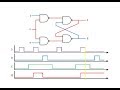
Understanding Gated SR Latches: Operation and Applications Explained
Explore how gated SR latches enhance control in digital circuits by enabling state changes only when permitted. This guide covers the design differences between NOR and NAND based gated SR latches, their timing behavior, and practical uses such as independent room cooling control in air conditioning systems.
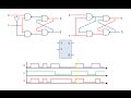
Understanding Gated Dlatches: One-Bit Memory Devices Explained
This article explains the construction and operation of gated Dlatches, built from gated SR latches, and explores their behavior using timing diagrams. Learn how Dlatches function as one-bit memory devices, their advantages over SR latches, and their applications in data storage and transfer.
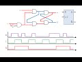
Understanding Clocked D Latches and Edge-Triggered Flip-Flops
Explore the operation and enhancements of clocked D latches, including edge detection for precise timing control. Learn how these devices synchronize data storage in digital circuits and their role in memory and counter applications.
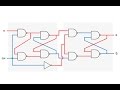
Master-Slave D-Type Flip-Flops: Ensuring Reliable Digital Circuit Timing
This summary explains the importance of clock synchronization in digital circuits and how propagation delays affect circuit stability. It details the design and function of master-slave D-type flip-flops, illustrating how they prevent glitches and ensure data integrity across clock cycles.

Understanding Boolean Functions: Sum of Products and Product of Sums
This video tutorial explains how to represent Boolean functions in both Sum of Products (SOP) and Product of Sums (POS) forms. It covers the concepts of minterms and maxterms, providing examples and clarifying the differences between canonical and non-canonical forms.
Most viewed summaries

A Comprehensive Guide to Using Stable Diffusion Forge UI
Explore the Stable Diffusion Forge UI, customizable settings, models, and more to enhance your image generation experience.

Kolonyalismo at Imperyalismo: Ang Kasaysayan ng Pagsakop sa Pilipinas
Tuklasin ang kasaysayan ng kolonyalismo at imperyalismo sa Pilipinas sa pamamagitan ni Ferdinand Magellan.

Mastering Inpainting with Stable Diffusion: Fix Mistakes and Enhance Your Images
Learn to fix mistakes and enhance images with Stable Diffusion's inpainting features effectively.

Pamamaraan at Patakarang Kolonyal ng mga Espanyol sa Pilipinas
Tuklasin ang mga pamamaraan at patakaran ng mga Espanyol sa Pilipinas, at ang epekto nito sa mga Pilipino.

How to Install and Configure Forge: A New Stable Diffusion Web UI
Learn to install and configure the new Forge web UI for Stable Diffusion, with tips on models and settings.
Found this summary useful?
Take it with you. One click puts it in your own LunaNotes library.
Save to LunaNotes