Introduction to Gated SR Latches
An SR latch is a fundamental memory device in digital electronics that stores a single bit of information. A gated SR latch extends this functionality by adding an enable input, ensuring the latch only changes state when enabled.
Practical Example: Independent Room Cooling
Imagine a building with individual cooling units controlled by separate SR latches, each receiving set/reset signals from temperature or humidity sensors. With gated SR latches, a central control panel can enable or disable each unit independently, providing precise environmental management.
Basic SR Latch Overview
- NOR-based SR latch: An active-high latch, requiring a high (1) pulse at the Set (S) or Reset (R) input to change the output (Q).
- Invalid condition: Both S and R inputs should not be high simultaneously as this causes an undefined state.
- Level sensitivity: Output changes as soon as inputs are at a valid logical level, regardless of pulse duration. For a deeper understanding of level sensitivity concepts, see Understanding Java Short Circuit Operations: A Comprehensive Guide.
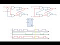
Creating a Gated SR Latch from a NOR-based Latch
- Add two AND gates in series with the S and R inputs.
- Introduce a new input E (Enable), controlling when the latch can change state.
- Output responds to S or R only if Enable (E) is high.
NAND-based SR Latch Characteristics
- Built from cross-coupled NAND gates.
- Active-low inputs: a low (0) pulse on S or R sets or resets the latch.
Modifying NAND SR Latch to Gated Version
- Add two extra NAND gates as 'steering gates,' yielding a third input E.
- Transforms an active-low latch into an active-high gated latch.
Behavior Differences: Transparent vs Gated
- Transparent (no steering gates): Inputs directly affect output at all times.
- Gated SR latch: Inputs affect output only when enable (E) is high.
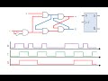
Symbol and Timing Diagrams
- Gated SR latches have specific symbols showing inputs S, R, E, and outputs Q and !Q.
- Timing diagrams help visualize output changes relative to input-level transitions over time. For an extended study of timing and AC circuit behaviors relevant to signal processing, consult Understanding LCR Circuits: A Guide to AC Circuit Theory.
- Digital signal levels: 0 V (logical 0) or ~5 V (logical 1).
Example Timing Insights
- When Enable is low, changes in S or R do not alter the output Q.
- When Enable is high, Q responds immediately to valid S or R pulses, following the characteristic latch behavior of holding state until the next change.
Summary
- NOR-based SR latches become gated by adding AND gates controlled by an enable signal.
- NAND-based SR latches become gated and shift from active-low to active-high by adding NAND steering gates.
- The enable input E ensures controlled, conditional state changes, making gated SR latches valuable for systems needing selective control.
- Timing diagrams and standard symbols aid in understanding and designing these latches for practical digital applications. For additional digital design concepts related to latch and flip-flop circuits, see Mastering Verilog: A Comprehensive Guide to Digital Design and Programming.
a gated set/reset latch is an SR latch that can only change state while it's enabled for example imagine an air
conditioning system in the building each room could have its own cooling unit controlled independently by its own
SR latch the set and reset signals might come from a temperature sensor or a humidity sensor in the room if these
were gated SR latches then a central control panel could be used to enable or disable the switching on and off of
these units on a room-by-room basis here's an uncoated SR latch remember an SR latch built from nor gates like this
one is an active high SR latch this means it requires a high pulse that's a 1 to be applied at input s in order to
get a high output at Q in other words to set the latch alternatively to reset the latch and make the output at Q 0 it
requires a high pulse to be applied to input R it's invalid for both s and R to be made high at the same time an SR
latch is said to be level sensitive this means it will respond to a valid change in either S or R regardless of the
duration of the input pulse it's the level high or low that matters not how long it's applied for to build a gated
SR latch we can make some simple enhancements to an SR latch by connecting a pair of and
gates in series with the inputs of an or based SR latch we've created a third input e which can be used to enable or
disable the latching effect a regular and gate will only have a high output if both inputs are high so only when e is
set to one with a one from s or a one from our get through to our cross connected nor gates here's an SR latch
built from NAND gates this is a of sensitive active low sr latch in other words both S&R are normally high
and it requires a low pulse that's a zero to be applied to s in order to set it it also requires a low pulse to be
applied to R in order to reset it by connecting an extra pair of NAND gates to the latch like this not only have we
created a third input e we now have a new circuit in which the normal states of s and r are zero and high pulses are
required to set or reset the latch in other words our NAND based latch has been changed from an active low latch
into an active high latch these additional gates on a basic SR latch are sometimes referred to as steering gates
an SR latch without steering gates is said to be transparent a valid input will affect the output unconditionally a
gated SR latch on the other hand is transparent only when it's enabled it's convenient to give a gated SR latch its
own symbol because we can now focus on what the latch does rather than what's going on inside it the inputs SE and r
are still shown and so is the output q and its inverse not cute we can illustrate what's going on at any
one of the inputs or the output on a chart showing changes in voltage against time at any given moment the voltage
will be either low zero volts to all intents and purposes and representing the binary value zero or high at about
five volts representing the binary value one now of course everything can happen very quickly in a digital circuit each
time interval on this chart could be in the order of a microsecond that's a millionth of a second
having said that for a level sensitive gated SR latch each time interval might be one second or one minute or even an
hour it really depends on the application for the purposes of this discussion it takes no time for the
voltage to change from low to high or from high to low in reality this transition takes a few nanoseconds the
significance of which we'll ignore for now but come back to in a later video let's proceed on the assumption that
switching from low to high or vice-versa is instantaneous this gives us the classic square wave that you can see
here we now have a convenient way to describe the behavior of a latch by stacking several charts together one for
each input SR D and one for the output Q with a common time axis we can visualize this circuit in action
at the time indicated by the vertical yellow line the output Q is low s and R are also both low but E is high so the
latch is enabled in fact in this diagram the latch is always enabled so it's going to behave exactly like a simple SR
latch without steering gates as time passes if s goes high so does Q because it's a latch when s
drops too low again Q stays high if s goes high while Q is high it has no effect Q is already high when R goes
high Q goes low when s goes high again so does Q this is normal latching behavior again we see our going
high so the latches reset again the latch is already reset so another
pulse it R has no effect now let's examine what happens when e varies you can see that some of the time he is high
and some of the time he is low we begin with an output of zero but Q and because he is low the latch is disabled s goes
high but it has no effect on the output of the latch now he is high the latch is enabled so when s goes high
so does Q and when there stops too low again the latch stays high until such time as R goes high and then Q drops to
zero again now he is zero the latch is no longer enabled so if s goes high it has no effect on queue
he is high again the latch is enabled and so it responds when s goes high the latch is set again he goes to zero the
latch is disabled R goes high but Q doesn't drop it remains in its high state to summarize then an SR latch
built from nor gates can be turned into a gated SR latch by adding a pair of and gates to it an SR latch built from NAND
gates can be turned into a gated SR latch by adding another pair of NAND gates to it this also has the effect of
changing the SR latch from an active low to an active high latch a gated SR latch has an additional input e which must be
high before the latch will respond to any changes in S or R the gated SR latch has its own symbol to simplify diagrams
and the behavior of a latch can be described by means of a timing diagram
A gated SR latch stores a single bit of information like a standard SR latch but includes an enable input (E) that controls when the latch can change its state. This ensures that the latch changes output only when enabled, allowing for more precise control in digital circuits.
In a NOR-based SR latch, adding an enable input involves placing two AND gates before the Set (S) and Reset (R) inputs. The latch responds to S or R signals only when the enable input (E) is high, preventing unintended state changes when E is low and thus providing conditional control over the latch's output.
NOR-based gated SR latches are active-high devices, meaning they respond to high signals on S or R inputs when enabled. NAND-based latches use active-low inputs, with low pulses on S or R triggering state changes. To gate a NAND latch, extra NAND gates are added as steering gates, transforming it into an active-high gated latch, allowing inputs to affect output only when enable is high.
Having both Set (S) and Reset (R) inputs high at the same time in a NOR-based SR latch leads to an invalid or undefined state where the output becomes unpredictable. This condition disrupts the reliable operation of the latch and should be avoided in practical circuit designs to maintain consistent behavior.
Timing diagrams visually represent changes in the inputs (S, R, and Enable) and the resulting output (Q) over time. They clearly show that when Enable is low, changes to S or R do not affect the output, whereas when Enable is high, valid inputs immediately alter the output. This helps designers verify correct operation and timing relationships in digital systems.
Gated SR latches are useful in systems requiring selective control of memory elements, such as controlling independent room cooling units with individual latches enabled by a central panel. The enable input allows precise environmental management by permitting state changes only when desired, improving system flexibility and efficiency.
To create a gated SR latch from a basic NOR SR latch, two AND gates are inserted in series with the S and R inputs, controlled by an enable signal (E). This modification ensures that S or R signals only affect the latch output when E is high, thereby gating the latch and preventing unintended changes when E is low.
Heads up!
This summary and transcript were automatically generated using AI with the Free YouTube Transcript Summary Tool by LunaNotes.
Generate a summary for freeRelated Summaries
Understanding Gated Dlatches: One-Bit Memory Devices Explained
This article explains the construction and operation of gated Dlatches, built from gated SR latches, and explores their behavior using timing diagrams. Learn how Dlatches function as one-bit memory devices, their advantages over SR latches, and their applications in data storage and transfer.
Understanding Clocked D Latches and Edge-Triggered Flip-Flops
Explore the operation and enhancements of clocked D latches, including edge detection for precise timing control. Learn how these devices synchronize data storage in digital circuits and their role in memory and counter applications.
Master-Slave D-Type Flip-Flops: Ensuring Reliable Digital Circuit Timing
This summary explains the importance of clock synchronization in digital circuits and how propagation delays affect circuit stability. It details the design and function of master-slave D-type flip-flops, illustrating how they prevent glitches and ensure data integrity across clock cycles.
Understanding MOS Junction C-V Characteristics: Accumulation, Depletion, and Inversion
Explore the intricacies of MOS junction C-V characteristics and their operational regimes: accumulation, depletion, and inversion.

Mastering Verilog: A Comprehensive Guide to Digital Design and Programming
Unlock the secrets of Verilog programming for digital systems. Learn from basics to advanced topics with ease!
Most Viewed Summaries

A Comprehensive Guide to Using Stable Diffusion Forge UI
Explore the Stable Diffusion Forge UI, customizable settings, models, and more to enhance your image generation experience.

Kolonyalismo at Imperyalismo: Ang Kasaysayan ng Pagsakop sa Pilipinas
Tuklasin ang kasaysayan ng kolonyalismo at imperyalismo sa Pilipinas sa pamamagitan ni Ferdinand Magellan.

Mastering Inpainting with Stable Diffusion: Fix Mistakes and Enhance Your Images
Learn to fix mistakes and enhance images with Stable Diffusion's inpainting features effectively.

Pamamaraan at Patakarang Kolonyal ng mga Espanyol sa Pilipinas
Tuklasin ang mga pamamaraan at patakaran ng mga Espanyol sa Pilipinas, at ang epekto nito sa mga Pilipino.

How to Install and Configure Forge: A New Stable Diffusion Web UI
Learn to install and configure the new Forge web UI for Stable Diffusion, with tips on models and settings.

If you found this summary useful, consider buying us a coffee. It would help us a lot!