What is a Gated Dlatch?
A gated Dlatch is a fundamental digital memory device capable of storing one bit of data. The "D" stands for "Data," emphasizing that it directly captures and holds input data.
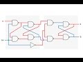
Construction from Gated SR Latch
- A gated SR latch uses NAND gates with inputs S (Set), R (Reset), and an enable signal E.
- Both S and R are normally low; a high pulse on either changes the latch state.
- When enabled (E high), the latch is "transparent" and outputs follow inputs. For more details, see Understanding Gated SR Latches: Operation and Applications Explained.
Problem with Gated SR Latch
- Simultaneously setting S=1 and R=1 leads to an invalid or forbidden state.
- This causes both Q and not Q outputs to be high, resulting in unpredictable behavior known as a race condition.
Dlatch Solution
- Invert the S input to create R = NOT(S), ensuring S and R are always complements.
- Rename S to D; this forms the gated Dlatch.
- Since S and R cannot be high simultaneously, forbidden states are eliminated.
Behavior of Dlatch
- When enable (E) is high, Q output follows D input.
- When enable (E) is low, Q holds its last state regardless of D changes.
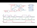
Alternative Dlatch Construction
- By rewiring four NAND gates cleverly, Dlatches can be implemented more efficiently, using fewer components.
- This design feeds the inverse of D internally, maintaining the complementary input relationship.
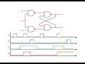
Timing Diagram Analysis
- Shows Q following D while E is high.
- When E switches low, Q retains its previous output value, effectively latching the data.
- Re-enabling E resumes Q tracking D. Understanding timing and signal behavior can be enhanced by exploring similar concepts discussed in Understanding K Map: A Simplified Guide to Karnaugh Maps.
Applications of Dlatches
- Used as one-bit memory elements in digital systems.
- Essential for converting parallel data streams into serial data via multiplexers.
- Commonly found in input/output ports for temporary data storage.
Latches vs Flip-Flops
- Though often confused, latches and flip-flops differ:
- Latches: Level-triggered, transparent when enabled.
- Flip-flops: Edge-triggered, change state at clock transitions.
- Latches serve as building blocks for flip-flops. To deepen your understanding of designing digital systems including flip-flops, refer to Mastering Verilog: A Comprehensive Guide to Digital Design and Programming.
This comprehensive understanding of gated Dlatches highlights their role as stable, simple memory devices that avoid the pitfalls of SR latches, enabling reliable data storage and manipulation in digital electronics.
A gated dlatch is a one-bit memory device. The D stands for data. A gated Dlatch is also referred to as a data
latch or simply a Dlatch. We're going to look at how a Dlatch can be built from a gated SR latch and examine its behavior
with a timing diagram. Let's first remind ourselves of a potential problem associated with gated
SR latches. Remember a gated SR latch can be constructed from NAND gates. A gated SR latch is an active high latch.
In other words, both S and R are normally at low voltage representing zeros. And a pulse is required at one of
these in order to set or reset the latch. Meanwhile, if the output at Q is high,
the latch is set and it's storing a one. But if Q is low, the latch is not set and it's storing a zero.
The gated SR latch has a third input E which when high enables the latch. The latch is said to be transparent when
it's enabled. As elegant as it is, we have a potential problem with this circuit.
There's a possibility that S and R could be made high simultaneously. This would be like asking the latch to
store a one and a zero at the same time, which is nonsense. In reality, both Q and not Q would become high. Then, if
both S and R fell to zero at the same time, we'd have a race condition. The cross-connected NAND gates would race
each other to feed back their outputs, making it impossible to predict the next state of the latch.
This would be like tossing a coin. the latch would end up in either one of its two stable states. Needless to say, this
kind of unpredictability in an electronic circuit is usually unacceptable.
So, what can we do about it? By simply inverting input S with a notgate, then feeding this notgate's
output into R so that R and S are always the opposite of each other, the forbidden input combination of S= 1 and
R= 1 can never be applied. Now we can rename input S to D. D for data. And now we have a oneinput gated
SR latch, otherwise known as a Dlatch. Let's see it in action. While E is high, if D is high, then so
is Q. While E is high, if D changes to low, then so does Q.
You can see that while E is high, Q is always the same as D. And because we're using a notgate like this, there's no
possibility of the Dlatch ever ending up in a forbidden state like an SR latch might.
This is still a latch, of course, because if E falls to zero, output Q will retain its previous value. And the
Dlatch will no longer respond to changes in D. It's locked in its current state. Let's return to our gated SR latch for a
moment. By cleverly rewiring the same four NAND gates like this, we've built a Dlatch in
a different way. It does exactly the same thing as the Dlatch that we built by using a notgate. But because we're
using less components, this version is more efficient and cheaper to make. Let's look at both designs together.
We can see that this new version is taking advantage of the fact that the output of the top NAND gate is always
the inverse of D as long as the latch is enabled. So this output is fed back into the lower gate. A rather elegant
solution. Let's quickly check it is indeed doing the same thing by tracing the highs and
lows through the gates again. At the moment E is high, D is high and so is Q. E is still high. D goes low. And so does
Q. E goes low. D and Q remain as they were low. E is still low. D becomes high. But Q
remains low. E becomes high again. D is already high. So Q goes high.
Now let's examine the behavior of a Dlatch on a timing diagram. This type of analysis might reveal some behavior we
haven't spotted yet. First though, we're going to give the Dlatch its own symbol so we can focus on what it does rather
than how it was built. We're interested in the relationship between D, E, and Q. So here they are on
a shared time axis. Not Q is always the inverse of Q. So we haven't included it on this diagram.
At our starting point, E is high. In other words, the Dlatch is enabled. D is low and therefore so is Q.
When D goes high, so does Q. When D goes low, so does Q. You can see that while E is high, Q is following D.
When E goes low, Q is latched. It can't change. So we can see here changes in D are not being
reflected in Q. D at the moment is low. Q is high. But when E goes high again, Q reflects D.
And once again Q is following D. On this diagram, we see E going low again. So Q is no longer following D
until of course E goes high again. To summarize then, a Dlatch, otherwise known as a data latch, can be built from
a gated SR latch, either by including a notgate or by simply rewiring the existing NAND gates.
Regardless of how it was built, the Dlatch has its own symbol and its behavior can be described on the timing
diagram. The essence of this behavior is that the output follows the input while the Dlatch is enabled. If the Dlatch is
disabled, it retains its current state. This means the Dlatch can be used to capture and store one bit of data. It's
a one bit memory device. Dlatches are useful for converting parallel data into serial data. A group
of Dlatches can hang on to several bits of data while a multipplexer accesses them one at a time and places them onto
a serial transmission line. Typically, Dlatches are found in input output ports.
One final point, latches are sometimes referred to as flip-flops, but strictly speaking this is not correct. Latch
circuitry does however form the basis of a flip-flop, and I'll be looking at these later.
A gated Dlatch is a basic digital memory device that stores one bit of data by capturing the input when the enable signal (E) is high. When enabled, the output Q follows the input D; when disabled, it holds the last value, effectively 'latching' the data until re-enabled.
The gated Dlatch fixes the forbidden or invalid state problem in gated SR latches by ensuring that the Set (S) and Reset (R) inputs are always complementary (R = NOT S). This eliminates the race condition caused by both S and R being high simultaneously, making the Dlatch more reliable for data storage.
When the enable signal E is high, the output Q tracks the input D, making the latch transparent. When E transitions from high to low, Q holds its last value regardless of changes in D, effectively storing the data. Re-enabling E resumes Q's following of D. This timing control is essential for synchronizing data storage in digital systems.
Gated Dlatches serve as one-bit memory units used in digital systems for temporary data storage, such as input/output ports. They are also vital in data conversion tasks, like converting parallel data into serial form via multiplexers, due to their simple and stable data holding properties.
Gated Dlatches are level-triggered devices that are transparent when enabled, meaning their outputs change as long as the enable is high. Flip-flops, on the other hand, are edge-triggered and only change output at clock signal transitions (rising or falling edge). Flip-flops are typically built using latches and are preferred for synchronous designs requiring precise timing.
Yes, a gated Dlatch can be implemented efficiently by rewiring four NAND gates so that the inverse of the D input is generated internally, maintaining complementary inputs without separate inverters. This method reduces component count and simplifies the circuit design while preserving proper latch behavior.
Heads up!
This summary and transcript were automatically generated using AI with the Free YouTube Transcript Summary Tool by LunaNotes.
Generate a summary for freeRelated Summaries
Understanding Gated SR Latches: Operation and Applications Explained
Explore how gated SR latches enhance control in digital circuits by enabling state changes only when permitted. This guide covers the design differences between NOR and NAND based gated SR latches, their timing behavior, and practical uses such as independent room cooling control in air conditioning systems.
Understanding Clocked D Latches and Edge-Triggered Flip-Flops
Explore the operation and enhancements of clocked D latches, including edge detection for precise timing control. Learn how these devices synchronize data storage in digital circuits and their role in memory and counter applications.
Master-Slave D-Type Flip-Flops: Ensuring Reliable Digital Circuit Timing
This summary explains the importance of clock synchronization in digital circuits and how propagation delays affect circuit stability. It details the design and function of master-slave D-type flip-flops, illustrating how they prevent glitches and ensure data integrity across clock cycles.

Understanding Computer Memory: RAM, ROM, HDD, SSD, and More
Explore the fundamental types of computer memory and storage, including RAM, ROM, HDD, SSD, and flash drives. Learn how each type functions, their advantages, and their role in computing performance.

Digital Electronics: Lecture 1 - Number Systems & Base Conversions for GATE 2025
Join Ankit Sir for the first lecture of his new Digital Electronics course for GATE 2025. This session covers the introduction to digital vs. analog signals, the critical importance of sampling and quantization, and the fundamentals of number systems including binary, octal, and hexadecimal, with a focus on base conversions.
Most Viewed Summaries

A Comprehensive Guide to Using Stable Diffusion Forge UI
Explore the Stable Diffusion Forge UI, customizable settings, models, and more to enhance your image generation experience.

Kolonyalismo at Imperyalismo: Ang Kasaysayan ng Pagsakop sa Pilipinas
Tuklasin ang kasaysayan ng kolonyalismo at imperyalismo sa Pilipinas sa pamamagitan ni Ferdinand Magellan.

Mastering Inpainting with Stable Diffusion: Fix Mistakes and Enhance Your Images
Learn to fix mistakes and enhance images with Stable Diffusion's inpainting features effectively.

Pamamaraan at Patakarang Kolonyal ng mga Espanyol sa Pilipinas
Tuklasin ang mga pamamaraan at patakaran ng mga Espanyol sa Pilipinas, at ang epekto nito sa mga Pilipino.

How to Install and Configure Forge: A New Stable Diffusion Web UI
Learn to install and configure the new Forge web UI for Stable Diffusion, with tips on models and settings.

If you found this summary useful, consider buying us a coffee. It would help us a lot!