Introduction
In recent lectures, we delved into the intricacies of MOS junctions and their capacitance-voltage (C-V) characteristics. This article aims to elucidate the concepts discussed, including accumulation, depletion, and inversion regimes of operation within MOS capacitors. Understanding these concepts is crucial for analyzing semiconductor devices and optimizing their performance in microelectronics.
Understanding the Basics
Before diving deeper into the C-V characteristics, we must establish some essential terms:
- Accumulation: This regime occurs when the gate voltage is below the flat-band voltage ( V_FB). The concentration of majority carriers at the interface increases, resulting in accumulation of charge.
- Depletion: When the gate voltage exceeds V_FB but is still below the threshold voltage ( V_T), majority carriers are depleted from the semiconductor surface, leading to a region with an overall negative charge.
- Inversion: Beyond the threshold voltage ( V_T), the majority carriers are effectively replaced by minority carriers, resulting in the formation of an inversion layer where the concentration of minority carriers dominates.
The C-V Characteristics Diagram
To graphically represent these regimes, we will define the electron concentration ( ns) and hole concentration ( ps) at the semiconductor interface. The bulk concentrations of electrons and holes will be denoted as n0 and p0, respectively. As illustrated in a typical C-V characteristics diagram:
- Accumulation: when n < n0
- Depletion: as n approaches n0
- Weak Inversion: when n > n0 but < p0
- Strong Inversion: when n ≥ p0
Transitioning from Log to Linear Scale
The discussion of charge density and electric field requires translating these characteristics onto a voltage scale. From the diagram explaining the various regimes, the point where n = p0 marks the threshold voltage (V_T). The importance of understanding the transition from a logarithmic scale to a linear scale cannot be overstated:
- Logarithmic Scale: Offers a broader view of charge dynamics across various regimes almost continuously.
- Linear Scale: Provides specific insights into shifts in concentration post-threshold.
Flat-band Voltage and Threshold Voltage
The concept of flat-band voltage ( V_FB) relates to the formation of a flat energy band diagram under equilibrium conditions, typically at V = 0 for an ideal capacitor. Understanding why this point is termed flat-band requires examining the energy bands:
- When V = 0, both the conduction and valence band edges are horizontal, reflecting uniform carrier concentrations across the semiconductor. Moreover, it is critical to note that the relationship between flat-band voltage and threshold voltage is significant.
- Flat-band voltage typically precedes the onset of depletion as the gate voltage exceeds V_FB.
Analyzing Depletion and Inversion Charges
As we investigate C-V characteristics beyond the threshold voltage, we discern distinct behaviors of depletion charge ( Q_d) and inversion charge ( Q_i):
- Depletion Charge ( Q_d): Increases with the voltage and tapers off beyond V_T, indicating that the depletion region reaches a saturation point. This behavior reflects the need for additional, mobilized charge from the electrons rather than a mere increase in depletion of holes.
- Inversion Charge ( Q_i): In contrast to Q_d, the inversion charge rises sharply once V_T is surpassed. As the MOSFET operates within the strong inversion regime, this charge governs the device's performance, significantly affecting its conductivity and threshold response.
Equations for Charge and Electric Field
The charge calculations involve distinct equations before and beyond threshold voltage conditions. Notably, beneath the inversion regime, the charge conditions evolve and require numerical analysis based on derived relationships:
-
For depletion condition: [ Q_d = - \epsilon_s E_s, ]
-
For inversion layer: [ Q_i = Q_{i0} \cdot e^{(V - V_T)/V_{Tn}} ]
These equations form the backbone of understanding charge dynamics within the MOS structure, underpinning crucial aspects of electrical behavior.
Conclusion
In conclusion, we have streamlined the understanding of MOS junction characteristics focusing on C-V behavior across accumulation, depletion, and inversion regimes. Recognizing these aspects is pivotal in semiconductor device design, enabling engineers to develop more efficient and effective applications in contemporary microelectronics. Through detailed analysis of charge conditions and voltage relationships, we establish a foundation for further exploring advanced topics in semiconductor theory and application.
As we proceed to our next class, we will derive expressions for Q_d and Q_i as functions of voltage to complete our exploration of the C-V characteristics of MOS capacitors.
In the last class we started our discussion on the MOS junction. We shall continue this discussion in this particular lecture.
You would recall that we have set the goal of explaining the C - V characteristics shown on this slide. Now what we achieved in the last class is that for an ideal MOS capacitor
we have explained the accumulation, depletion and inversion regimes of operation. We can show these various regimes of operation on a simple diagram. So let us draw a line indicating the various conditions in the semiconductor
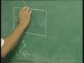
as far as the electron concentration at the interface is concerned. So this shows ns on a log scale. What is ns? If these are the hole and electron concentrations for any voltage this quantity
is ns and this quantity is ps and this bulk concentration of electrons we will denote as n0. Now suppose this is n0 this is ni and this is p0, so p0 is this, the bulk concentration of holes.
We can identify the regimes of operation in terms of these concentrations. When your n is less than n0 that is this regime you have accumulation. When n starts becoming more than n0 or correspondingly the hole concentrations starts becoming less
than p0 therefore here you have depletion. Now this depletion continues until your ns = p0. Now in this region you can separate and you can identify a weak inversion region when
your ns is more than ni but less than p0. So this is the weak inversion. Just as depletion implies removal of majority carriers Inversion is nothing but the pile up of minority carriers so that they dominate the bulk majority carriers.
So whatever be the amount of majority carriers present in the bulk they are dominated by the minority carriers at the interface.. So at the interface the minority carriers in the bulk are really the majority carriers because they are dominating.
Therefore weak inversion and beyond ns = p0 here you have strong inversions. Now, in our first course what we said is that we will call this region as the inversion region. Whenever we use the word inversion it would imply strong inversion.
The treatment of weak inversion is more complex so that is taken up in advanced courses on semiconductor devices. Now what is it that distinguishes strong inversion from weak inversion?
The pile up of the electron charge at the interface as shown in this diagram that is this area starts becoming significant in the strong inversion region. Now we can translate this diagram that you are able to see also to the voltage axis.
For example, in terms of voltage if you show this is V the gate voltage, then this point when ns becomes equal to p0 is said to be the threshold point and this voltage is called the threshold voltage. On the other hand this point where the surface
concentration of the electrons is same as the bulk concentration or when the charge conditions in the device is 0 it is normally referred to as the Flat-band voltage. So this translates to this point in terms of the voltage, the conditions in the device
translating to terminal voltage and this translates to threshold voltage point. Let us understand why this point is called the Flat-band point. To understand this we need to draw the energy band diagram for that condition.
So this condition is also the condition V = 0 for an ideal capacitor. So VFB = 0 for ideal capacitor. So what is this Flat-band and what is the meaning of this Flat-band?
So, if I draw the energy band diagram in the semiconductor for V = 0 which is a Flat-band for an ideal capacitor you will find that the conduction band edge and valance band edge both of these edges are flat they are horizontal.
That is because there is no variation in the hole or electron concentration as a function of X for V = 0. So recall that the hole concentration is flat and electron concentration is flat for V = 0. So this flat hole and electron concentration
conditions translate to flatness of the conduction and valance band edges and therefore this condition is called the Flat-band condition. Please note that we are considering a uniformly doped substrate. If the substrate is non-uniformly doped then
even when voltage is 0 the doping will result in a non-uniform hole concentration and electron concentration and then the bands will not be flat. So for our case we understand why the voltage equal to 0 condition is referred to as the
Flat-band condition. So accumulation implies voltage less than VFB. From VFB to VT this is the depletion region and for gate voltage beyond VT you have the inversion region.
Now we need to find out what is this threshold voltage. We already know that the Flat-band voltage for an ideal capacitor is 0. Now, for this purpose we need to translate our hole and electron distributions in the
semiconductor to charge an electric field condition. For the threshold condition the hole concentration is shown here as 4 and electron concentration also has been shown. It turns out that this electron concentration
that is the area under the electron distribution is really small compared to the charge because of depletion of holes. So we can neglect this charge under threshold voltage conditions that is at threshold voltage conditions.
If that being the case we can draw the charge on electric field conditions as follows: So this our hole concentration on a linear scale. Now we draw the space charge. Since the charge is negative we draw it on the negative side. So that is the space charge where this value
here is - q(Na) approximately. We know from our PN junction theory that in depletion layer this space charge concentration is - q times the ionized impurity concentration and we are assuming complete ionization.
Now we will assume the depletion approximation. That is, we will assume that this region has an abrupt ending for simplicity of analysis. Now based on this we can sketch the electric field. The electric field is on the positive axis
because the electric field is positive from left to right, this charge is negative. Since this space charge is constant here be Gauss's law we will get a straight line for the electric field up to the interface. Now what happens in the oxide?
When you move from one region to another region of different dielectric constant then the electric fields on the two sides of the boundary are related by the formula epsilon 1 E1 = epsilon 2 E2 so these are the two electric fields this is E1 this is E2 and the dielectric constants
are epsilon 1 and epsilon 2. Now, using this particular relation if you call this as the surface electric field in semiconductor, that is, we give the symbol Es here.
In terms of this we can draw the electric field in the oxide. So in the oxide layer the electric field would be a constant because there is no space charge and this electric field would be related to this electric field by this formula.
So we can substitute the dielectric constants here and then we will find, this is Eox therefore this is epsilon ox and here it is epsilon silicon and this is Es. So from here we have Eox = Es × epsilon silicon/epsilon ox.
Epsilon silicon is 12 and epsilon ox is 4 = 3(Es). Therefore you take three times this and that is your Eox filled in the oxide. Now what happens in the metal or gate? Obviously you have the opposite charge so
here you have the charge shown by a delta function on the positive side because you have a positive charge. So the electric field will abruptly drop to 0 in a small distance. The field is not of interest because it falls
abruptly in the metal. Now this area under the electric field distribution is the applied voltage and that is the threshold voltage. So to know the threshold voltage we need know this area.
Now let us identify the components of the applied voltage across oxide and across semiconductor on the electric field versus x diagram. So here this area is a voltage drop across the oxide that will indicate as si ox.
On the hand this area is a voltage across semiconductor and this we will denote as si s. So let us see in terms of our capacitor. What are these components? Now you are applying a voltage here and this voltage is falling across the oxide
and across the semiconductor, this is the applied voltage V. So, in general you have V = si ox + si s. Now we need to identify si ox and si s, we need to get the values. Now it is interesting to note that you can
get si s from the hole and electron concentrations versus distance diagram at threshold. So at threshold your concentrations of electrons and holes are as follows: So ns = p0 that is a point here, this is hole concentration and this is electron concentration
at threshold. You can use Boltzmann relation because this semiconductor is under equilibrium. So Boltzmann relation gives you the potential drop in this region if there is a variation as shown here.
Now this value here is n0 and that is p0. So this is si s the potential drop in the semiconductor which can be written as Vt × lawn of the concentration here that is ns/concentration in the bulk that is n0 which is nothing but Vt lawn p0/n0 this is the Boltzmann relation.
Now we can simplify this equation because we know we can write n0 in terms of p0 so this is nothing but Vt × lawn of p0/ni2/p0 because p0 n0 is ni2 which will then be simplified to two times Vt × lawn of p0/nI so that is your si s.
So si s = 2Vt lawn p0/ni. Now we know what is p0? p0 is approximately the doping of the substrate. Therefore p0 is approximately equal to Na. Therefore we have the relation, si s is approximately 2Vt lawn Na/ni.
In other words we know the value of si s at threshold in terms of the substrate doping. So this is si s at threshold. In other words we have identified this area here.
Please note that the si s will vary with voltage. We are talking about the conditions right at the threshold. Now once we know this we know this area also because we know this Eox is three times Es because of the dielectric constants of silicon
being 12 and oxide being 4. Therefore now we can write an equation for threshold as follows: So threshold voltage = si ox + 2Vt lawn Na/ni where si ox is Eox × t0 = 3Es × t0 because Eox is 3Es.
And for Es you have a relation. This area is 2Vt lawn Na/ni but this area we can write in terms Es and doping level itself using our analysis we did for PN junction. So for Es your relation is half of Es × the depletion width Xd, the depletion width Xd
is this. So this is 2Vt lawn Na/ni. Now this Xd we can again write in terms of the charge so this Xd is nothing but the depletion charge which we denote as Qd. We are putting a modulus because the depletion charge is negative.
What is the depletion charge? Let us look at this diagram, this is the depletion charge Qd. Of course at threshold this also happens to be the charge in the semiconductor qs but that is a different issue. So now Xd is Qd/doping
× q. And this Qd and Es are related by Gauss's law. That is, this Es and this Qd, so what is the relation? The relation is Qd = epsilon s × Es but Es is positive and the charge is negative.
So Qd is - epsilon s Es so modulus of Qd is epsilon s Es. Here in this formula you can write this Qd/QNa as epsilon s Es/QNa so that now you can replace Xd in terms of epsilon s and you have the relation, 1/2 Es2/qNa × epsilon s. This is the left hand side so this is equal
to 2Vt lawn Na/ni. Now let us indicate this particular voltage which is coming often with a symbol so that we do not have to write this whole term. Let us call this voltage as phi t that is the surface potential at threshold.
Note that the potential drop in the semiconductor si s found here is also referred to as surface potential because this si s is the potential of this point with respect to the bulk and this is this surface and that is why it is called surface potential. We are assuming
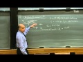
that the bulk potential is 0 in the semiconductor, reference. From here we can derive the following formula for Es; Es = √2q Na phi t/epsilon s. Now we can substitute this value of Es here and therefore get this si ox.
And we will get the expression for threshold as VT = 3t0 × √2q Na phi t/epsilon s + phi t. Now this three is nothing but the ratio of the dielectric constants of semiconductor and
oxide. So we can simplify by writing this 3 as epsilon s/epsilon ox and then we can cancel these terms and shift this epsilon s to the numerator and epsilon ox/t0 is the so called oxide capacitance
C0. So we can write this formula as √2q Na phi t epsilon s/C0 + phi t where phi t is given by this 2Vt lawn Na/ni. Now this is the equation, let us write it completely.
So this is the equation for threshold voltage of an ideal MOS capacitor. We have on the right hand side all the material parameters. So basically you see it depends on the doping level Na the temperature t because that decides
ni and Vt and the oxide thickness which decides the C0. Of course you also have the dielectric constants coming in there. Now in this form you can identify the particular term the first term on the right hand side
that is this term as follows: Since this is the dimension of holes the numerator is charge by unit area because charge by unit area divided by capacitance per unit area will give you voltage. Now here what is the charge we are talking about? This charge is
nothing but this particular depletion charge here. So this is identified as Qd at inversion with a modulus because the charge is negative. Now this is again charge per unit area. We need to emphasize that the area we are talking
about is perpendicular to the board. That is, the area is perpendicular to this. Now what does these Qd/C0 term indicate? It is like the voltage across the insulator of a parallel plate capacitor having charge Q.
That is how this formula is very easy to remember. In this formula this is the potential drop in the oxide which is given by the parallel plate capacitor formula charge on the electrode of the oxide that is the semiconductor divided by the capacitance and this is the voltage
drop in silicon. Therefore voltage drop in silicon plus the voltage drop in oxide at threshold you sum up and then you get the threshold voltage. Now it is useful to get some feel for what
kind of values we get for the threshold voltage. So we will do a solved example. The solved example is: Calculate the threshold voltage of an ideal MOS capacitor having the following parameters: p-substrate doping level of 1.45 × 10¹⁶/cm3
and oxide thickness of 0.2 micrometre. That is t0 = 0.2µm and the temperature is 300 K. Basically these are the parameters corresponding to the experimental C - V curve we showed which we are going to explain.
Let us start using this formula. If you substitute the various parameters what kind of values we get for the two terms on the right hand side. Let us calculate phi t first. phi t at 300
K is 2 ×0.026 volts × logarithm of 1.45 ×10¹⁶/1.5 ×1010. Now after calculating you find that this is approximately 106. So when you take log of 106 the 6 will come out and you will have lawn 10.
So that 6 gets multiplied by 2 and you have 12 so twelve times 0.026 × lawn 10. It turns out that this quantity will be about .72 volts. So this phi t value is somewhat like the value of the built in voltage of a PN junction about
.7. Now the next quantity to calculate is this C0 which is capacitance of the oxide per unit area. So C0 is epsilon ox/t0 which
is 4 × 8.85 × 10-14/0.2 × 10-4 F/cm/cm. So you see the capacitance is F/cm2. Now this value will be of the order of Nano Farad's because this 10-4 goes up and then you have 10-10 but then you have .2 here
so multiply numerator and denominator by 10 and this will become 2 and here you will have 10-9. So this value is 17.7 nF/cm2. Now it is useful to remember the typical value of C0 like we remember the typical value of
phi t which is about .7. Now please note that phi t is logarithmly dependent on the doping level here. So even if the doping level changes the value of phi t does not change very significantly.
You will find it will remain between .6 and .8 volts so .7 is a good value to remember. Similarly for C0 we find that for 0.2 micron thickness oxide the capacitance is 17.7 nF/cm2. It is useful to remember the value for 0.1 micrometer because 0.2 micrometer is not so
easy to remember but relatively it is easier to remember the 0.1 micrometer thickness which is same as 1000 Angstroms in terms of Angstroms. Whenever you are handling small geometries you must be very comfortable with dimensions of the order of Angstroms and microns and
you must be able to convert one from the other. So 0.1 micron oxide thickness is equal to 1000 Angstroms. So for this 1000 Angstroms oxide thickness your C0 would be double the value that you
have obtained for 0.2 microns because the capacitance is inversely proportional to the oxide thickness. So, for this the C0 is approximately 35.5 nF/cm2. So one remembers this value for t0 = 0.1 microns or 1000 Angstroms this is the capacitance.
So, in practice whenever you come across any other oxide thickness you can always calculate the capacitance of that particular MOS capacitor by scaling the oxide thickness in appropriate manner starting with this value.
Next we need to calculate the numerator of this equation. Now we can write √2q Na epsilon s × phi t/C0 = √2 × 1.6 × 10-19. We always collect all powers of 10 together and we also write the units here Coulomb.
Then doping level is 1.45 × 10¹⁶ so we put that here and this is for cm3. Then comes epsilon s. You recall from calculations done for PN junction that approximately we can assume the epsilon s to be 10-12 F/cm for silicon.
Basically this value 10-12 for epsilon is given by 12 × 8.85 × 10-14 because dielectric constant of silicon is 12. And then you have to multiply by phi t that is .72 so 0.72 so we will shift this to the right a little bit and this into 10-19+16-12
and F/cm is volts. Now this divided by C0 is 17.7 ×10⁻⁹ so this is F/cm2 So you have centimetre square in the numerator and Farad in the denominator. Now let us first check the units here.
So this is coulomb and Farad in to volt is also coulomb. And now Coulomb square and cm power 4 in the denominator, so this centimetre power four in the denominator becomes centimetre square when it comes out of the square root and this
becomes coulomb. So this is the unit so coulomb by Farad is nothing but volts. Dimensionally this equation is correct and we need to evaluate it numerically.
So here you will find you have powers of 16 - 12 = 4 - 19 + 4 = 10-15. Now you can make it 10-16 and multiply this quantity on this side by 10 so that what you get out from the square root is 10-8. Now bottom is 1.77 × 10⁻⁸.
So10-8 and 10-8 will cancel so you will get this of the order of volts. It turns out that this value is equal to 3.26 volts. Now you sum up 3.26 volts and .72 volts and you get VT = 3.26 + .72 that is 3.98 volts
that is about 4V. So you find that about 4 volts is the threshold voltage. That is the voltage you must apply to the MOS capacitor that is this voltage in order
to achieve threshold voltage conditions in the semiconductor. Out of this approximate value of 4 volts please note that only about .7 is falling in the semiconductor that is this value here phi t is the si s potential drop in the semiconductor
and this is potential drop in the oxide. So you find that most of the applied voltage falls across the oxide and a very small value falls across the semiconductor. Now let us proceed further and see what happens beyond threshold because in fact from the
point of view of operation of a MOSFET we will find that it is a regime beyond threshold that is of significant interest. So let us plot the concentrations in the p-type substrate for voltages beyond threshold. So it is V greater than VT and supposing you
vary this voltage what is going to happen? First start from the threshold voltage point this is p0, this is n0 so this is the hole concentration, this is the electron concentration at threshold. Beyond threshold what happens
is this concentration rises even beyond this p0 value and this will obviously fall. Now, this point is the so called intrinsic point because here the hole and electron concentrations are equal and therefore they will be equal to ni.
You will recall from the PN junction depletion region analysis that even there you had an intrinsic point. Now, coming back to the concentrations, this is electrons and these are holes you find that ns is now more than p0. Now what is interesting
to note is that you will find that this depletion edge will not change very significantly beyond threshold. Here this is the edge of the depletion layer. This is an important point that we must understand that the depletion region almost ceases to
expand beyond the threshold voltage point. Let us see why. Let us plot these same concentrations on a linear scale. This is the hole concentration and this is the electron concentration at threshold
but beyond threshold this is somewhere here the electron concentration is like this. This is when you plot on the linear scale. Please note that this is on a log scale whereas this is on a linear scale. To understand why the depletion region does
not expand significantly beyond threshold you must plot this concentration on a linear scale. And there you find that even a small charge here on the log scale in the electron concentration
means a large change in the linear scale. This is almost a factor of 10, in fact we have not shown a factor of 10 increase here. If you really want to show a factor of 10 increase then this concentration should have been shown somewhere here or even beyond.
So we are not able to show it to scale. The point is that, now if you see this area under this curve this is going to rise rapidly beyond threshold. Therefore whenever you apply extra voltage you need extra charge in the semiconductor
and beyond threshold what is happening is that the extra charge is coming from these electrons. The extra charge comes more easily from the electrons rather than by depleting the holes and exposing the negatively charged acceptor
impurities. So until the capacitor reaches the threshold when you increase the voltage the extra negative charge required in the semiconductor comes from the ionized impurities by expanding the depletion layer.
But once you reach the threshold and go beyond this whenever you increase the voltage beyond threshold the extra negative charge required in the semiconductor comes from the mobile electrons which are very close to the surface. And since this mobile concentration now can
increase very rapidly there is no need to expand the depletion layer to provide for this negative charge. Now these aspects can be shown nicely on a graph. In fact one can do numerical calculation of this situation.
The analysis of this to find out this particular charge under this area is not a straight forward analysis but it requires some intense numerical calculations because you have to solve a number of complicated equations. But we can sketch the graph qualitatively
to show what is happening here. So for that purpose we will translate this diagram on to a space charge versus distance diagram. So if you translate this diagram to space charge versus x this is how it looks.
At threshold this is your space charge so rho versus x. And you are not able to show any electron charge here so this is that electron charge that is very small at threshold.
But beyond threshold there is a very slight increase here but here the increase is very high. The dashed line shows beyond threshold. If you recall curve number 4 was threshold
voltage so let us call this curve number 5. You should connect this diagram to the diagram we had drawn for carrier concentrations for voltage conditions below threshold then you
will understand why this is 4 and this is 5. So here this white is 4 and this is 5. So 4 corresponds to V = VT and 5 corresponds to V greater than VT. So this is the charge we are talking about. So now you need not have to increase this
area under this rectangle to get the charge. The extra charge beyond threshold comes from increase in this negative charge because of electrons. What we will do is we will call this area under the electrons or the electron charge
as the inversion charge and denote it by the symbol Qi. Now the charge of electrons is negative so we will put a modulus here because this area is positive. Similarly we will show the space charge because of electrons by a separate delta function here. This is like
a delta function where it is showing electrons as a sheet of charge so this is Qi. Please note that space charge is on a negative axis and this area is the depletion charge. Now we sketch Qi and Qd as a function of voltage. As I have said earlier the calculation for
Qi and Qd for V greater than VT will have to be done numerically. We are only presenting the results here and based on it we can make a very simple approximation and we can get the charge conditions and calculate them.
As a function of V supposing this is the threshold voltage point and this is the origin of Flat-band voltage then your depletion charge goes on increasing like this and almost saturates beyond this threshold voltage. So there is a small increase but the rate of increase
is very small beyond this. So this is Qd. On the other hand if you sketch this Qi as a function of voltage you will get it is as follows. If Qi is very small up to threshold and beyond threshold it starts increasing rapidly, so this is Qi this is the threshold
voltage point. This is the depletion region and beyond this you have the inversion region. Now we can complete the picture and show the accumulation charge on the other side. When your voltage is negative you have accumulation
charge. Recall that the relationship between accumulation charges and voltage is a straight line and that charge is positive. So this is Q accumulation, suffix a stands for accumulation. The silicon charge stands for sum of Qd and
Qi because this total thing is the silicon charge. So if you want to sketch the silicon charge that would look something like this and that we will show by dotted line, so this dotted line is Qs.
Here of course the Qs and Qa are the same. Here the Qs is obtained by summing up these two. So beyond threshold it is almost Qi and below threshold it is almost Qd so that is the charge condition.
Now this explains why or how the depletion region stops expanding beyond threshold because with increase in voltage the extra charge in semiconductor comes from the mobile electrons and you are getting an inversion layer. Now, what we want to do is to derive expressions
for Qi and Qd as a function of voltage. We already have an expression for Qa as a function of voltage. So when you have expressions for Qd and Qi versus voltage we have the complete QV characteristics. So what we have drawn here is actually the QV characteristics that
we wanted to derive for the MOS capacitor. So this is a charge in silicon versus the voltage. In the next class we will derive the equations for Qd and Qi as a function of voltage. Now here to complete the explanation let us
see what happens to the potential drop in silicon because we said the applied voltage drops across silicon and oxide. At threshold we have seen that si s = phi t that is about .7V. Now what happens beyond
threshold? Since the depletion charge is almost saturating or the depletion layer is almost saturating what we find is that the surface potential or the potential drop in silicon psi s also almost saturates at the value corresponding
to the threshold voltage. So if you sketch si s as a function of voltage you will find the variation to be something like this. For V = 0 si s is 0. At threshold it is phi t and beyond threshold it almost saturates
at phi t. There is a small increase but that increase is very small. Therefore in inversion we can assume no matter what the voltage is so long as it is beyond threshold the surface potential is approximately equal to phi t.
Heads up!
This summary and transcript were automatically generated using AI with the Free YouTube Transcript Summary Tool by LunaNotes.
Generate a summary for freeRelated Summaries
Understanding Metal Oxide Semiconductor Capacitance and Voltage Characteristics
Explore the intricate details of MOS capacitors, their voltage characteristics, and implications of non-ideality.
Understanding Conductors and Capacitors in Electric Circuits
Explore the critical concepts of conductors, capacitors, and electric circuits in this comprehensive guide.
Understanding Circuits: Key Concepts and Theories
Explore the fundamentals of electrical circuits, current flow, and more with this in-depth guide.
MOSFET Large Signal and Small Signal Models: Analysis and Biasing
This lecture by Behzad Razavi explains the transition from large-signal to small-signal MOSFET models for amplifier design. It covers transconductance (GM) expressions, the importance of proper biasing, and how to use linear small-signal models for simplified analysis.
Understanding Electric Potential, Fields, and Capacitors in Physics
Explore electric potential, fields, and the role of capacitors in energy storage.
Most Viewed Summaries

A Comprehensive Guide to Using Stable Diffusion Forge UI
Explore the Stable Diffusion Forge UI, customizable settings, models, and more to enhance your image generation experience.

Kolonyalismo at Imperyalismo: Ang Kasaysayan ng Pagsakop sa Pilipinas
Tuklasin ang kasaysayan ng kolonyalismo at imperyalismo sa Pilipinas sa pamamagitan ni Ferdinand Magellan.

Mastering Inpainting with Stable Diffusion: Fix Mistakes and Enhance Your Images
Learn to fix mistakes and enhance images with Stable Diffusion's inpainting features effectively.

Pamamaraan at Patakarang Kolonyal ng mga Espanyol sa Pilipinas
Tuklasin ang mga pamamaraan at patakaran ng mga Espanyol sa Pilipinas, at ang epekto nito sa mga Pilipino.

How to Install and Configure Forge: A New Stable Diffusion Web UI
Learn to install and configure the new Forge web UI for Stable Diffusion, with tips on models and settings.

If you found this summary useful, consider buying us a coffee. It would help us a lot!