Introduction to Circuit Timing and Propagation Delays
Digital computers comprise hundreds of circuits, each with thousands of components interconnected with numerous dependencies. Signals traveling through these circuits experience propagation delays due to the inherent reaction times of logic gates and physical wire lengths. These delays vary based on factors such as temperature and manufacturing differences.
Impact of Propagation Delays
- Logic gates require finite time to respond to input changes
- Signal paths can involve thousands of gates
- Resulting glitches or unwanted fluctuations may cause temporary incorrect outputs
- Timing becomes critical especially in sequential circuits, where outputs depend on prior states
The Role of Clock Signals in Synchronization
To manage complexity and timing issues, a central clock signal synchronizes the operations of multiple components, analogous to a conductor coordinating an orchestra. This clock:
- Sets a common timing reference
- Ensures components work in harmony
- Enables predictable system behavior
One-Bit Memory Cells and Latches
A basic memory unit is a one-bit latch, which ideally stores input upon a clock transition. However, due to glitches from propagation delays, these latches may temporarily hold incorrect values if the clock cycle is too short or inputs change during crucial periods.
Challenges
- Glitches cause transient incorrect states
- Clock speed must balance faster operation against adequate settling time
- Edge-triggered pulse latches mitigate some issues but have limitations due to extremely short transition times
To understand these one-bit memory devices better, see Understanding Gated Dlatches: One-Bit Memory Devices Explained.
Master-Slave D-Type Flip-Flop Architecture
To overcome these timing challenges, a master-slave D-type flip-flop combines two level-triggered latches:
Components
- Master latch: Enabled when the clock is high; captures input data
- Slave latch: Enabled when the clock is low; outputs the stored data
Operation
- During the clock high phase, the master latch samples input D.
- The slave latch is disabled, preventing output change.
- When the clock transitions low, the slave latch is enabled and takes the master's output as its input.
- The flip-flop's output updates, ensuring signals do not pass directly through and eliminating glitches.
For deeper insight into the behavior and comparison with latches, refer to Understanding Clocked D Latches and Edge-Triggered Flip-Flops.
Timing Diagram Analysis
- The master follows input D only when clock is high.
- The slave follows the master only when the clock goes low.
- This gating arrangement acts like an airlock, preventing input changes from immediately affecting output.
- The input must be stable before clock rising edge and not change during the high phase to avoid glitches.
- The output updates are delayed by half a clock cycle, providing time for inputs to settle.
Advantages and Trade-offs
Benefits
- Immunity to glitches caused by input fluctuations during clock phases
- Controlled timing ensures reliable data transfer between sequential circuits
- Enables coordinated system operation based on clock cycles
Considerations
- More complex with higher component count than simpler latches
- Relatively slower operation and increased power consumption
For practical applications and design examples using hardware description languages, consult Mastering Verilog: A Comprehensive Guide to Digital Design and Programming.
Summary
Master-slave D-type flip-flops are fundamental one-bit memory devices in digital sequential logic. By combining two complementary, level-triggered latches with opposite clock phases, they provide stable, glitch-resistant outputs synchronized to a common clock. This design accommodates propagation delays and timing uncertainties, ensuring coherent behavior across complex digital systems.
there are hundreds of circuits inside a digital computer each type doing a particular
job some of these circuits include thousands of components working together so needless to say there's a huge number
of dependencies between these components the outputs of some being the inputs of many
others there are also many different paths a signal can take as it propagates through a system some of these paths
involving thousands of logic gates each gate takes time to react to changes in its inputs its so-called propagation
delay wires and connections also have propagation delays so the time it takes for a signal to travel around a circuit
depends very much on the path it takes and this isn't entirely predictable propagation delays depend on
factors such as temperature and variations in the manufacturing processes of electronic
components if a particular logic gate has received one correct input but is still waiting for another input to
arrive its output could be momentarily wrong and as you can imagine if this isn't controlled in some way there'll be
chaos in a sequential digital circuit timing is a fundamental consideration think about just one
example a circuit designed to keep count each input signal increments the counter by one each new Total depends
not only on the input signal but also on the counter's previous output so clearly when the input signal happens is
crucial this is why we need clocks with a clock the workings of several components can be synchronized
to just one signal rather like the condu of an orchestra a clock sets the pace and allows the components of a circuit
to work in harmony with each other and with other circuits the result is a system whose
behavior is more predictable let's consider a group of simple onebit memory cells in a register
controlled by a clock these are latches ideally to synchronize the setting of these latches we'd make all
of the puts the way we want them to be while the clock signal is low then when the clock signal becomes
High these input values would be transmitted to the latches and their values
stored but unwanted fluctuations can occur on the data lines because of propagation delays these are called
glitches and conceivably we can have a situation in which our latches haven't had enough time to achieve their correct
values before the clock pulse ends it's crucial that these inputs are allowed to settle into their correct
values while the clock signal is high why because no doubt there's a different circuit ready to make immediate use of
the data in the register perhaps during the very next clock cycle the outputs of these latches have
to be stable before they're sampled the data in this register has to be accurate before something else reads
it we could try to avoid the problem caused by glitches by speeding up the clock
allowing less time for them to matter but we also have to allow time for the components to do their jobs we have to
cater for their propagation delays if a clock's running too quickly some components won't be able to keep up we
can also make circuits less susceptible to glitches by building Edge triggered devices like pulse latches but the
rising edge of a clock cycle is in the order of only few Nan seconds and again even with very careful design there
might not be enough time for everything to keep Pace when choosing a clock frequency
that would allow this register to function correctly an engineer has to think about all of the circuitry
involved in generating the inputs the clock period must be such that all of the other circuits have time to
stabilize during the same high phase of the same clock cycle as I said by the time we get to
the next clock cycle when a different circuit needs to sample the output of each memory cell that output has to be
fixed if all of the circuits in a coordinated system work on the basis that only one signal change per clock
cycle matters then their behavior can be coordinated
reliably one way we can help to ensure that this is the case is to build a memory device that's immune to glitches
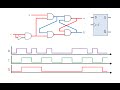
the so-called Master Slave dtype flip-flop here we have a level triggered gated D
latch and a level triggered gated Sr latch both of these latches are active High let's put the two together so that
the outputs of the D latch become the inputs of the SR latch let's rename the enabling input of
the D lch to CLK because this is going to be connected to a clock and now let's connect the inverse
of the clock signal to the enabling input of the SR latch this device is known as a Master
Slave dtype flipflop with this type of memory device we can precisely control the moment at
which a group of them will change State the latch on the left is is called the master and the latch on the right is
known as the slave the master latch reads the input value at D when the clock signal is high
and latches onto it in fact this begins to happen at the rising edge of the clock
cycle meanwhile the slave is disabled so the new output from the flip-flop as a whole is not available just
yet then when the clock signal Falls to low again the slave is enabled data is passed from the master to the slave and
is therefore available at the output a dtype flip-flop can be compared to an airlock consisting of two doors
which are never open at the same time the flip-flop as a whole is never fully open so an input signal can't pass
straight through as it does with a simple D latch the output of the flip-flop occurs during the next phase
of the same clock cycle as that in which the input occurred that is ever so slightly later the dtype flip-flop is
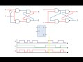
therefore sometimes referred to as a delay type flip-flop let's simplify our diagram and
analyze the behavior of a dtype flip-flop on a timing diagram we'll call the output of the
master qm and that of the slave Qs here's a timing diagram we'll focus first on D C and
qm the first thing you'll see is that the master behaves exactly like a gated DCH well of course it does because
that's exactly what it is qm follows D when the clock signal is high here C is high D is low and
therefore qm is also low the out of the master follows its input while C is high here D has become High presumably
because we want the output at qm to go high but because C is low this doesn't happen just yet qm stays low for now qm
only follows D when C is high the master is currently latched in a low State when C does go high again qm
reacts immediately to follow D qm is now High here when C goes low again D is
high and so is qm so the master is now latched in a high State now d goes low again presumably
because we want to change the state of the master latch back to low again but because C is low qm doesn't follow not
just yet and when C does go high again qm immediately goes low to follow d but now we can see D changing again
while the clock is high suppose for a moment that a completely different circuit depended on the output of qm
being low it may well have missed its chance to read the correct value suppose on the other hand a completely different
circuit depended on the output of qm being high then there's the possibility that it might read the wrong value
because it's reading it too soon unintended input fluctuations can be
problematic ideally the value of D should be set before the clock goes high and D should not change again during the
same high phase of the same clock cycle now C has gone low again and the master is latched in a high
State qm continues to follow D while C is high a couple of Cycles later and we can
see that the value of D is changing again during the high phase of the same clock cycle another glitch not
ideal now let's take a look at Qs the output of the slave and therefore the output of the flip-flop as a
whole Qs follows qm because the Master's output is the slave's input but more importantly Qs only follows qm while C
is low because the slave is being fed the inverse of the clock signal consider this point in time qm is
changing from low to high but Qs remains low because C is high while a flip-flop is responding to
a change in its input its output remains unchanged at this point in time however Qs becomes High to follow qm at the
falling edge of the clock sign notice that qm the Master's output cannot be changed now because C is
low this means that changes to the input of the flip-flop cannot impact on the output at this point also notice that
the output of the flip-flop has been delayed by half a clock cycle here the input at D has changed to
low as if in Readiness for another change to the state of the flip-flop when C go go high the output
of the master changes but this has no impact on Qs that is no impact on the output of the flip-flop as a whole the
slave isn't listening and soon after we see D going high again during the high phase of the
clock cycle but this glitch has no effect on the output of the flip-flop at this point we do see Qs
changing again to follow D while the clock signal is low but of course the master will ignore any changes in the
input while the flip-flops new output is being made available here we see that D has gone high as if to set the state of
the flip-flop to high on the next high pulse of the clock and when the clock goes High the Master's output qm follows
D but now the input Falls to low while the clock is high and so does qm so by the time the clock signal Falls
to low again and the slave is once again responding to changes in its input the flip-flop has ignored yet another
glitch what we've seen then is that the dtype flip-flop effectively ignores any input
fluctuations because the master and the slave are enabled on opposite phases of the same clock
cycle the flip-flop accepts input when the clock signal goes high but only gives up the corresponding output when
the clock signal Falls to low to summarize then a dtype flip-flop is a one bit memory
device several flip-flops can be combined to build a register or a bank of
memory a dtype flip-flop is built by combining two level triggered latches which act as a master and a
slave the output of the master is the input of the slave a dtype flip-flop is safe
because it allows sufficient time for propagation delays and therefore time for the inputs to change and settle down
without affecting the output a dtype flip-flop does however involve a lot of components compared to
say a pulse latch which makes it relatively slow and power hungry
Propagation delays occur because logic gates and physical wires take finite time to respond and transmit signals, varying with temperature and manufacturing variations. These delays can cause transient glitches in outputs, making timing critical especially in sequential circuits where outputs depend on previous states. Managing these delays ensures circuits function reliably and predictably.
A clock signal provides a common timing reference that coordinates when all components update their states simultaneously. By acting like a conductor, the clock ensures components operate in harmony, enabling predictable behavior and reducing timing errors caused by propagation delays and asynchronous inputs.
One-bit latches sample inputs when enabled, but due to propagation delays and input changes during critical periods, they can temporarily hold incorrect values or glitches. If the clock cycle is too short or inputs are unstable during latch activation, outputs may fluctuate undesirably, compromising reliability.
It uses two level-triggered latches—the master is enabled when the clock is high to sample input data, while the slave is enabled when the clock is low to output the stored data. This gating prevents direct signal flow through both immediately, effectively acting like an airlock that blocks glitches and ensures stable, glitch-free outputs synchronized to the clock.
The input signal should be stable before the rising edge of the clock and remain unchanged during the high clock phase to prevent glitches. Since the flip-flop updates output only after the clock transitions low, inputs must settle reliably within this timeframe for correct sampling.
Advantages include immunity to glitches, reliable and synchronized data transfer, and enabling coordinated sequential operations. Trade-offs involve increased circuit complexity, slower speed compared to simpler latches, and higher power consumption due to additional components and switching activity.
Practical design examples and applications using hardware description languages like Verilog can be found in resources such as "Mastering Verilog: A Comprehensive Guide to Digital Design and Programming." These materials provide detailed guidance on coding, simulation, and integration of flip-flops in complex digital systems.
Heads up!
This summary and transcript were automatically generated using AI with the Free YouTube Transcript Summary Tool by LunaNotes.
Generate a summary for freeRelated Summaries
Understanding Clocked D Latches and Edge-Triggered Flip-Flops
Explore the operation and enhancements of clocked D latches, including edge detection for precise timing control. Learn how these devices synchronize data storage in digital circuits and their role in memory and counter applications.
Understanding Gated Dlatches: One-Bit Memory Devices Explained
This article explains the construction and operation of gated Dlatches, built from gated SR latches, and explores their behavior using timing diagrams. Learn how Dlatches function as one-bit memory devices, their advantages over SR latches, and their applications in data storage and transfer.
Understanding Gated SR Latches: Operation and Applications Explained
Explore how gated SR latches enhance control in digital circuits by enabling state changes only when permitted. This guide covers the design differences between NOR and NAND based gated SR latches, their timing behavior, and practical uses such as independent room cooling control in air conditioning systems.

Mastering Verilog: A Comprehensive Guide to Digital Design and Programming
Unlock the secrets of Verilog programming for digital systems. Learn from basics to advanced topics with ease!

Understanding Snooping Based Cache Coherence Protocol Explained
Explore the detailed working principles of the snooping based cache coherence protocol, including its role in maintaining uniformity across processors. This session covers cache states, read/write strategies, and real-world applications in modern multiprocessors.
Most Viewed Summaries

A Comprehensive Guide to Using Stable Diffusion Forge UI
Explore the Stable Diffusion Forge UI, customizable settings, models, and more to enhance your image generation experience.

Kolonyalismo at Imperyalismo: Ang Kasaysayan ng Pagsakop sa Pilipinas
Tuklasin ang kasaysayan ng kolonyalismo at imperyalismo sa Pilipinas sa pamamagitan ni Ferdinand Magellan.

Mastering Inpainting with Stable Diffusion: Fix Mistakes and Enhance Your Images
Learn to fix mistakes and enhance images with Stable Diffusion's inpainting features effectively.

Pamamaraan at Patakarang Kolonyal ng mga Espanyol sa Pilipinas
Tuklasin ang mga pamamaraan at patakaran ng mga Espanyol sa Pilipinas, at ang epekto nito sa mga Pilipino.

How to Install and Configure Forge: A New Stable Diffusion Web UI
Learn to install and configure the new Forge web UI for Stable Diffusion, with tips on models and settings.

If you found this summary useful, consider buying us a coffee. It would help us a lot!