Introduction to High-Frequency Limitations in Conventional Tubes
When operating at microwave frequencies (above 1 GHz), conventional vacuum tubes experience several limitations:
1. Lead Inductance and Inter-Electrode Capacitance
- Increased capacitance and inductance at high frequencies raise the real part of input admittance.
- This reduces the operating frequency and affects performance.
- Mitigation: Reduce lead length and electrode area to minimize these effects.
2. Transit Time Effect
- Transit time is the electron travel time between cathode and anode.
- At microwave frequencies, long transit times cause electron oscillations and possible electron return to cathode.
- Mitigation: Accelerate electrons with high DC voltage and use velocity modulation.
3. Gain-Bandwidth Product Limitation
- Gain increases near resonance but bandwidth decreases since gain-bandwidth product is constant.
- Mitigation: Use re-entrant cavities or slow-wave structures.
4. Radio Frequency (RF) Losses
- High frequencies confine current to smaller conductor areas, increasing losses.
- Mitigation: Use larger conductors.
5. Dielectric Losses
- Insulating materials like glass envelopes cause dielectric losses.
- Mitigation: Reduce glass surface area.
6. Radiation Losses
- Wires approaching the wavelength emit radiation, reducing efficiency.
- Mitigation: Proper shielding to prevent radiation.
Classification of Microwave Tubes
Microwave tubes fall into two categories:
1. Cross-Field (M-Type) Tubes
- DC magnetic and electric fields are perpendicular.
- Electron motion is perpendicular to both fields.
- Example: Magnetron.
2. Linear Beam (O-Type) Tubes
- DC magnetic and electric fields are parallel.
- Electron beam aligns with both fields.
- Examples: Klystron, Traveling Wave Tube (TWT).
Two Cavity Klystron Amplifier
Construction
- Contains two cavities: an input (buncher) cavity and an output (catcher) cavity.
- Electron beam emitted by cathode and focused by electrodes.
- Drift space separates the two cavities.
- RF input voltage applied at the input cavity.
- Collector at output side with positive voltage.
Operation
- Without RF input, electron velocity and spacing remain uniform.
- RF input causes velocity modulation:
- Electrons experience varying acceleration depending on RF voltage phase.
- Faster electrons overtake slower ones during drift space, forming electron bunches.
- Bunches reach output cavity and induce amplified RF output.
- Amplification results from energy transfer via bunching process.
Numerical Example: Calculation of Input Voltage, Output Voltage, and Power Delivered
Given:
- Voltage gain = 10 dB
- Input power = 5 mW
- Input shunt resistance (R_shin) = 30 kΩ
- Output shunt resistance (R_shout) = 40 kΩ
Step 1: Calculate Input Voltage (V_in)
- Formula: P_in = V_in2 / R_shin
- V_in = sqrt(P_in × R_shin) = sqrt(5 × 10−3 × 30 × 103) ≈ 122.47 V
Step 2: Calculate Output Voltage (V_out)
- Voltage gain (dB) = 20 log(V_out / V_in)
- 10 = 20 log(V_out / 122.47), thus log(V_out / 122.47) = 0.5
- V_out / 122.47 = 10^{0.5} = 3.162
- V_out ≈ 122.47 × 3.162 ≈ 387.28 V
Step 3: Calculate Power Delivered to Load (P_load)
- P_load = V_out2 / R_shout
- P_load = (387.28)2 / (40 × 103) ≈ 3.75 W
Conclusion
Understanding the high-frequency limitations in conventional tubes is critical for efficient microwave amplifier design. The two cavity Klystron amplifier overcomes these limitations through electron velocity modulation and bunching mechanisms, enabling effective amplification at microwave frequencies. The numerical example demonstrates practical calculation methods for key amplifier parameters.
For a deeper understanding of capacitance effects relevant to tuning and frequency response in such microwave circuits, consider reading Understanding Metal Oxide Semiconductor Capacitance and Voltage Characteristics.
Additionally, insights into resonant cavity behavior and quality factors can be complemented by exploring Understanding MOS Junction C-V Characteristics: Accumulation, Depletion, and Inversion.
To further grasp high-frequency circuit components impacting amplifier design, Understanding Inductors in Circuit Theory: A Deep Dive also offers valuable context on inductance, which is critical in addressing lead inductance issues discussed earlier.
hello and welcome you all dear students today's topic is two cavity KRON amplifier before uh discussing this
working and construction of a two cavity Clon amplifier first let us discuss the high frequency HF means high frequency
high frequency limitations of the conventional tubes from the exam point of view you may expect the question like
this what are high frequency limitations of the conventional tubes and how these liit itations can be overcome or can be
minimized so first limitation is lead inductance and Inter electrode capacitance effect there are different
electrodes between which the capacitance is created as well as the leads are present so it it produces certain effect
that is the lead inductance effect as the frequency increases we know that microwave is having a very high
frequency so as the frequency increases especially if frequency becomes more than 1 GHz then the capacitance between
the electrodes of a vacuum tube and the lead inductance of a wire goes on increasing this upward Arrow indicates
values goes on increasing in case of high frequencies the real part of input admittance re
means real part real part of the input admittance is very very large so the operating frequency of the tube goes on
reducing it affects the performance of a tube remedy uh to this problem to this limitation is reduce the lead length as
well as reduce the electrode area so it will reduce down the effect of lead inductance and Inter electrode
capacitance second limitation is Transit time effect Transit time is the time taken by the electrons uh to move from
cathode to anode the transit time is doned by notation to it is given by D by V 0 where small D is the distance
between anode and cathode V 0 is the velocity of electrons at micro frequency this Transit time is large so electrons
can ulate back and forth and it may happen that some of the electrons May return back to the cathode So to avoid
this or to minimize this effect accelerate Electron Beam with a high DC voltage and it should be followed by the
voltage by the velocity modulation process third limitation is gain bandwidth product the gain bandwidth is
having a fixed value at the higher frequencies that is at the uh micro frequencies and particularly at the
resonance condition the gain of device is increased but gain is increased and gain bandwidth product is fixed so it
will reduceed on the bandwidth of the device so So to avoid such limitations to minimize this limitation use
re-entrant cavities or you may use slow W structure it will reduce down the uh speed so fourth limitation is RF losses
radio frequency losses at the higher frequencies the current which is flowing through the circuit is confined to a
very small cross-sectional area so as the frequency increases this type of losses RF losses goes on
increasing this can be avoided by increasing the size of the conductor fifth type of limitation is dialectric
losses we know that uh different types of insulating materials are used for example glass envelopes are used which
causes dialectric losses so to reduce down uh this dialectric loss effect or this limitation reduce the surface area
of the glass and last type of limitation is radiation losses whenever the dimensions of a wire approaches towards
wavelength Lambda then the radiation starts that means the wire starts emitting the radiation it will affect
the performance of the uh circuit as well as it will reduce down the efficiency to avoid radiation losses
there should be a proper sing so this is about the high frequency limitations of the conventional tube and how to
minimize this effect So to avoid all these limitations we are going to make use of some microwave tubes
next part is classification of micro tubes the broad classification is there are two types of micro tubes one is
cross filled tubes it is also called M type tubes and another is linear beam tubes which is also called O type tubes
in case of Cross Field or M type tubes as the name indicates the fields are crossed that means in this case the DC
magnetic field and DC electric field are perpendicular to each other as well as the motion of electrons is also
perpendicular to both these things that is both to both DC magnetic and DC electric field so three things DC
electric field DC magnetic field and the motion of electrons are mutually perpendicular to each other so it is
called Crossfield microwave tubes examples are magnetron or Crossfield devices second type is linear beam tube
or O type of tube in this case the DC magnetic field is in parallel with DC electric field and the Electron Beam is
aligned with both these fields examples are KRON then twt that is traveling W tubes and so on as such we are going to
study all these devices uh in detail in this unit next part is two cavity Clon
amplifier let us first discuss the construction of two cavity Clon amplifier from the exam point of view
you may expect the like this draw the constructional details of two cavi Clon amplifier and explain its operation so
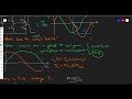
this diagram shows the construction of two cavity Chron amplifier as the name indicates there are two cavities one at
the input side this is called input cavity or buncher cavity second cavity is at the output side it is output
cavity or it is also called catcher cavity now this this part shows the cathode
which is used to emit the Electron Beam the focusing electrodes are placed on both sides of this cathode which are
used to focus the beam of electrons which is generated by the cathode now this part is the part of the
glass tube at the output side collector is shown more positive voltage is applied to the collector end now the gap
of input cavity is denoted by X and gap of output cavity is denoted by y the gap between the two cavities is called Drift
space in between these two cavities the different electron bunches are created now the RF input voltage is applied at
this point I mean is applied at the input cavity which is shown in this diagram now let us discuss the operation
of this two cavity Clon amplifier as I said the cathode is used to emit the Electron
Beam the drift space is gap between input and output cavities initially uh whenever input is
not applied basically this RF input is applied at the input cavity that is Bucher
cavity this input is to be Amplified now if RF input is not applied then look at this initial lines actually if each line
is having certain slope this line represents distance between X and Y this is X at the output cavity we have
written y so distance between them uh is called the drift space so each L represents the distance between X and Y
if initially RF input signal is not applied then observe these initial lines the slope remains constant there is no
change in the slope of these lines now consider one electron B see this is the voltage vform this electron B can be
treated as a reference electron this electron B is transferred whenever the voltage is slightly positive so because
of this the slope of the line gets changed as I said consider this as a reference electron now consider one more
electron that is electron C electron B is passed through the cavity after that electron C enters because electron C is
having more positive voltage compared to electron B since the volage of electron C is more than that of B the
acceleration of electron C takes place compared to electron B so slope of the line this line corresponding to or
compared to the line of related to electron B will be different will be changed that means make it more
simper whenever the voltage is high compared to the voltage at electron voltage of electron B so acceleration of
this electron takes place compared to the motion of electron B consider one more electron a which is passed when the
voltage is negative for this electron the acceleration will be minimum because
this electron is at the negative cycle negative half cycle so there is a difference between
the acceleration provided to each electron depending on the position of the input or position of the voltage at
which these electrons are passing through the Gap so the point is that certain electrons are traveling with
high speed certain electrons are traveling with low speed this electron a was transmitted earlier before passing
of el Elon B and C the acceleration of electron B is more than a acceleration of electron C is more than b as well as
more than a so it may happen that in between this Gap in the drift space the uh slower electrons will be captured
will be catched by the faster electron so different bunches are created this is called the bunching process so these
different bunches are shown in this diagram now all these bunches are formed due to the fast and slow motion of the
corresponding electrons whenever the bunches are formed faster electrons transfer energy to the slower electron
and all these bunches are captured in the output cavity that is catcher cavity and from this point the output is
generated so this is how the amplification process takes place basically amplification takes place due
to the formation of different bunches or due to the bunching process so this is about the working of two cavity Clon
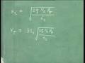
amplifier now let us solve a numerical given question is two cavity Clon amplifier has following characteristics
voltage gain which is given in DB it is 10 DB input power 5 mwatt shun resist impedance of input cavity that is rsh of
input cavity is 30 kilo then same CH impedance of output cavity 40 kilm total output impedance the notations can
notation can be r0 or RN so it is 40 Kil determine input voltage second part output voltage third part power deliver
to the load I have written the corresponding formula so first is input power is expressed as V in square that
is square of input voltage upon rsh for input power for at input side so this is at input side now we are supposed to
calculate input voltage initially so from this formula I can write v² is = p in into rsh of the input side now input
power is given as 5 m so it is 5 m means 5 into 10us 3 given value is in m so I have converted it into WS into rsh at
input side so rsh of input cavity is 30 30 kilm so it is 30 into 10 3 so you'll get value of v in square but
actually we need V in so take square root of this term this 10us 3 10 + 3 gets cancelled so square root of 150
will give you answer 12247 volt this is the answer of first part now for the second part we have the
formula of voltage gain 20 log V upon v0 upon V in do remember the voltage gain is given in DB so the corresponding
equation is 20 log of this ratio now let us put the values so in this equation a that is voltage gain is this value is
given in the question which is 10 DB so I can write 10 is = 20 log of v0 upon just now we have calculated value of V
that is 12247 so I can write it like this log of v0 upon
12247 is equal to 10 by 20 that is equals to.5 therefore v0 upon
12247 is anti log of5 therefore v0 is equals to I will
transfer this 12247 at the rhs side so it becomes 12247 into 10 to.5 because it is anti-log so answer of v0 is
38728 volt this is the answer of second part that is the answer of output voltage now third part power deliver to
the load we have SIMPLE formula V 0 squ upon RL the notation can be RL or r0 so PL I will get it as v0 squ that is
this value 38.78 squ upon RL 40 K that is 40 into 10 3 so this gives me the value of out
power deliver to the load which is .375 wat you may well convert it in mwatts that will be 37.5 M so this is
the way how to solve the uh for two cavity clone amplifier so dear students that's it for today's
session so thank you thanks a lot for watching this video
Conventional vacuum tubes face several limitations at microwave frequencies above 1 GHz, including increased lead inductance and inter-electrode capacitance that degrade input admittance, transit time effects causing electron oscillations, gain-bandwidth product constraints that reduce bandwidth, higher RF losses due to skin effect, dielectric losses from insulating materials, and radiation losses from wires approaching the wavelength. Mitigating these involves design changes like reducing lead lengths, using high DC acceleration voltages, employing specialized cavity structures, larger conductors, minimizing glass envelope areas, and shielding to prevent radiation.
The two cavity Klystron uses velocity modulation and electron bunching for amplification. An input RF voltage applied at the first cavity modulates the velocity of the electron beam emitted by the cathode; faster electrons catch up with slower ones during the drift space, forming dense electron bunches. These bunches induce an amplified RF signal in the output (catcher) cavity, effectively transferring energy from the electron beam to the RF field and producing amplification at microwave frequencies.
To minimize lead inductance and inter-electrode capacitance—which degrade performance at high frequencies—designers reduce the physical lead length and electrode area. Shorter leads lower inductance, and smaller electrode surfaces decrease capacitance. These measures improve the real part of input admittance, allowing the tube to operate effectively at microwave frequencies.
Given input power, input shunt resistance, output shunt resistance, and voltage gain in dB, you can calculate the input voltage V_in using V_in = √(P_in × R_shin). Then, calculate output voltage V_out using the voltage gain relation: Gain(dB) = 20 log(V_out / V_in). Finally, compute the power delivered to the load as P_load = V_out² / R_shout. For example, with 5 mW input power, 30 kΩ input shunt resistance, 40 kΩ output shunt resistance, and 10 dB gain, V_in ≈ 122.47 V, V_out ≈ 387.28 V, and P_load ≈ 3.75 W.
Microwave tubes are classified mainly into cross-field (M-type) tubes and linear beam (O-type) tubes. Cross-field tubes, like magnetrons, have perpendicular DC magnetic and electric fields causing electron motion perpendicular to both fields. Linear beam tubes, such as Klystrons and Traveling Wave Tubes (TWTs), have parallel electric and magnetic fields with the electron beam aligned along these fields. The operational principles and electron dynamics differ accordingly, influencing their application in microwave amplification.
Velocity modulation is crucial because it initiates electron bunching necessary for amplification. By applying an RF input voltage, electrons are accelerated to varying velocities based on the phase of the input signal. During the drift space between cavities, faster electrons catch up to slower ones, forming concentrated bunches that transfer energy efficiently in the output cavity, resulting in an amplified RF signal. Without velocity modulation, electron spacing remains uniform and no amplification occurs.
To reduce RF losses caused by the skin effect, using larger conductor cross-sections helps confine currents less restrictively and decreases resistance. To mitigate dielectric losses, minimizing the surface area of insulating materials like glass envelopes reduces energy dissipation. Additionally, careful material selection for lower loss tangents and effective shielding to prevent radiation losses enhance overall efficiency of microwave tubes.
Heads up!
This summary and transcript were automatically generated using AI with the Free YouTube Transcript Summary Tool by LunaNotes.
Generate a summary for freeRelated Summaries
Understanding Resonant Converters: Inverter and Rectifier Modeling Explained
This video provides a detailed exploration of resonant converters, focusing on their construction, operation, and modeling. Key topics include the role of inverters, resonant networks, and rectifiers, with an emphasis on first harmonic approximation and the distinction between current-driven and voltage-driven rectifiers for efficient DC-DC conversion.

Understanding LCR Circuits: A Guide to AC Circuit Theory
Learn about LCR circuits, AC current, and the application of complex numbers in circuit analysis.

Understanding Sound Absorption Measurement with an Impedance Tube
Discover how to measure sound absorption using advanced impedance tube technology. Learn the setup, calibration, and analysis steps!
Understanding MOS Junction C-V Characteristics: Accumulation, Depletion, and Inversion
Explore the intricacies of MOS junction C-V characteristics and their operational regimes: accumulation, depletion, and inversion.
Understanding Inductors in Circuit Theory: A Deep Dive
Explore the complexities of inductors in circuit theory with this comprehensive guide.
Most Viewed Summaries

A Comprehensive Guide to Using Stable Diffusion Forge UI
Explore the Stable Diffusion Forge UI, customizable settings, models, and more to enhance your image generation experience.

Kolonyalismo at Imperyalismo: Ang Kasaysayan ng Pagsakop sa Pilipinas
Tuklasin ang kasaysayan ng kolonyalismo at imperyalismo sa Pilipinas sa pamamagitan ni Ferdinand Magellan.

Mastering Inpainting with Stable Diffusion: Fix Mistakes and Enhance Your Images
Learn to fix mistakes and enhance images with Stable Diffusion's inpainting features effectively.

Pamamaraan at Patakarang Kolonyal ng mga Espanyol sa Pilipinas
Tuklasin ang mga pamamaraan at patakaran ng mga Espanyol sa Pilipinas, at ang epekto nito sa mga Pilipino.

How to Install and Configure Forge: A New Stable Diffusion Web UI
Learn to install and configure the new Forge web UI for Stable Diffusion, with tips on models and settings.

If you found this summary useful, consider buying us a coffee. It would help us a lot!