Introduction
Metal Oxide Semiconductor (MOS) capacitors are fundamental components in modern electronics, playing a crucial role in devices such as transistors, diodes, and memory cells. Understanding their charge-voltage (C-V) characteristics is essential for engineers and scientists working in semiconductor physics. This article delves into the mechanisms behind the C-V characteristics of MOS capacitors, explaining critical concepts such as depletion and inversion regions and the effects of non-ideality on their performance.
The Basics of MOS Capacitors
What is a MOS Capacitor?
A MOS capacitor consists of three layers—metal (often polysilicon), oxide (typically silicon dioxide), and semiconductor (silicon). The device's behavior is influenced significantly by the charges present within these layers and their respective capacitances.
Charge Conditions in MOS Capacitors
When a direct current (DC) voltage is applied across the capacitator, the charge distribution in the semiconductor changes according to the applied voltage. Fundamental conditions include:
- Depletion Region: When a positive voltage is applied, it creates a depletion layer by repelling holes in a p-type semiconductor, resulting in a charge deficit near the oxide-semiconductor interface.
- Inversion Layer: Further increasing the voltage beyond a certain threshold (VT) leads to the accumulation of free electrons near the surface, forming an inversion layer.
These processes delineate the movement of major charge carriers and significantly impact the capacitance and voltage characteristics of the device.
Charge-Voltage Relationship
The C-V Characteristics
The C-V characteristics are essential for understanding how the capacitance of a MOS capacitor varies with applied voltage. This relationship is influenced by two primary charge components:
- Depletion Charge (QD): The charge in the depletion region, which is approximately constant up to the threshold.
- Inversion Charge (Qi): The charge due to mobile electrons attracted to the surface after inversion begins.
Key Equations
The following equations illustrate the charge-voltage relationships:
- For the Depletion Region:
[ V = -\frac{Q_D}{C} + S_S ]
Where ( S_S ) is the surface potential. - For the Inversion Condition:
[ V - V_T = -\frac{Q_I}{C} ]
Here, ( Q_I ) represents the inversion charge.
Graphical Representation of C-V Characteristics
Graphing the equations yields sections corresponding to accumulation, depletion, and inversion regions, showcasing how capacitance varies dramatically in these regimes. Understanding these sections enables better design choices in semiconductor devices.
The Non-Ideal MOS Capacitor
Introduction to Non-Ideal Effects
Real-world MOS capacitors are not ideal; several factors complicate their behavior. Among these are interface traps and fixed charges, which can alter the expected performance dramatically.
Flatband Voltage (Vfb)
In a non-ideal MOS capacitor, you start with a flatband voltage that deviates from zero due to fixed charge (Qf) present at the oxide-semiconductor interface. The applied voltage required to create zero charge conditions is now represented by:
[ V_{fb} = -\frac{Q_f}{C} ]
This expression highlights the impact of fixed charge on threshold voltages and flatband voltage.
Understanding Work Function Difference (Фms)
The work function difference (Фms) also significantly impacts the capacitor's operation. This difference arises from the varied energy levels between the metal and semiconductor, leading to the requirement of an additional flatband voltage to establish charge equilibrium.
Combined Effect of Qf and Фms
The overall flatband voltage, taking into account both Qf and Фms, can be expressed as:
[ V_{fb} = Ф_m - Ф_s - \frac{Q_f}{C} ]
This equation allows engineers to understand how both fixed charge and work function differences shift the zero charge condition and threshold voltage.
Conclusion
A thorough understanding of MOS capacitors, particularly their charge-voltage characteristics, is vital for design and analysis in semiconductor applications. The complexities arising from non-ideal behaviors, including interface traps and fixed charges, necessitate careful consideration during device development. By comprehensively analyzing these characteristics, engineers can optimize the performance of their electronic devices, ensuring reliability and effectiveness in practical applications.
The critical takeaway from this discussion is that voltage applied to a MOS capacitor influences not just the charge conditions within the semiconductor, but also modifies the essential parameters defining the capacitor's performance. Going forward, further exploration of material characteristics and fabrication techniques will continue to enhance the functionality and applicability of MOS devices across various technologies.
[Music] [Music] oh sh
on me [Music] in the last few lectures we have been
discussing about the metal oxide semiconductor Junction or
capacitor we shall continue this discussion in this lecture let me remind you that our goal
of these discussions on this topic is to explain the CV characteristics shown on this
slide we are coming closer to this explanation as a first step we said that we will explain the charge conditions in
the MOs capacitor as a function of the DC applied voltage and from there we will derive the CV
characteristics in the last class what what we explained was the following in a MOS
capacitor when your voltage is greater than zero you have depletion and inversion
conditions and we discussed these conditions in detail and said the following when you increase the voltage
from zero first the depletion region starts expanding the charge in the
semiconductor required to sustain this high voltage uh sustain this applied voltage
comes from the depletion region okay because of ionized impurity atoms now this proceeds
until you reach the threshold Beyond threshold what happens is this depletion region stops expanding and instead you
have mobile electrons being attracted to the surface in large numbers and Beyond threshold it is this mobile electron
concentration or inversion layer charge concentration that goes on increasing and the depletion layer
concentration saturates now this was shown on a graph like
this so here the depletion charge is saturating and the inversion charge Qi is rapidly expanding beyond the
threshold point we also said that if you look at the
voltages scox and SS that is the potential drop across oxide and silicon
as two components of the applied voltage then when you increase the voltage from zero
sco keeps monotonically increasing now C also increases in the beginning but beyond threshold voltage
when the depletion layer almost saturates the Cs also saturates so this is what we said about CS the surface
potential Beyond threshold it saturates to a value 5
t Okay the saturation is approximate of course whereas the sco keeps increasing continuously because the Silicon charge
as a whole which is some of the inversion charge and the depletion charge that keeps increasing though the
depletion charge saturates Beyond threshold now we also derived an expression for VT and as well as this
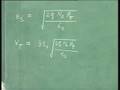
ft now this expression was VT = to < tk2 Q na Epsilon s 5T by C which is oxide capacitance plus 5 this
is the scox and this is CS at inversion we must remember two numerical values for any calculation related to
Moss capacitors one is the oxide capacitance for .1 Micron oxide thickness which is about 35.5 nanofarad
per cm square and the f t is approximately 7 volts it would be useful to remember
these two values now in this lecture we would like to derive expressions
for QD as a function of voltage and Qi as a function of voltage that is our first exercise in this lecture now
before we take that up let me explain one doubt that students often get that is how is it
that the cus almost saturates when your inversion charge is increasing that is the doubt is when you increase the
voltage Beyond threshold this electron concentration is going on increasing so NS is going on
increasing now if NS is going on increasing how can CS be
constant you know that we had said that Cs and ns are related by the bman relation SS
is equal to VT long NS by n that
is if you look at this diagram SS is given by the ratio of this surface
concentration to n KN and logarithm of this ratio multiplied by the threshold voltage so if n s
increases s should also increase but we are saying C is almost becoming constant how is this possible well what we are
saying is the following that c depends logarithmically on NS so even if NS increases the increase in C will be very
very small because NS is logarithmic function of uh the C is logarithmic function of NS on the other hand if you
look at the inversion charge Qi it increases almost linearly with NS the function is not
exactly linear but approximately we can say if that function of the function SS of NS is logarithmic this is almost
linear Qi is linear function of this NS so when NS increases Qi increases directly with NS
whereas C increases logarithmically with NS that is why even though the inversion charge increases rapidly the surface po
itial increases very slowly and therefore we are treating it as a constant now let us return to our
discussion related to derivation of equations for QD and Qi now the starting point for this is the same
as that we used for deriving the special voltage expression so we can
write V is equal to sco plus SS sco is given
by minus the Silicon charge by the oxide capacitance this is from the
field picture okay please note that Qs by c not with a minus sign because when the applied voltage is positive the
charge in the Silicon is negative charge in the Silicon is of opposite polarity to the voltage applied to the gate that
is why you have minus so this is generally true now depletion as well as inversion
so in um in the expression for Qs you will have QD as well as
Qi look at this graph we said the Q silicon silicon charge is obtained by summing up Qi and QD
so let us understand this with the help of a field versus distance
diagram now so we draw the E versus X okay in the oxide and semiconductor so at
threshold suppose this is the field distribution so this is four in our
nomenclature now Beyond threshold what happens is that you have a step in the electric
field here because you have the inversion charge which is almost like a
sheet and then your oxide electric field will be three times this electric
field so this in inversion this step is
Qi by Epsilon s with a modulus or you can put a negative sign because the charge is
negative this is by gs's law so the inversion charge contributes to a step in the electric field so we can draw the
charge picture here underneath this is the depletion charge under depletion approximation and this is the
inversion charge we are not showing the charge in the metal is always positive whenever
this charge is negative so corresponding to this sheet charge you have this
step this on the other hand this distance is minus QD by Epsilon
s so this total thing is Qs by Epsilon s with a negative sign
silicon charge by Epsilon S as you go on increasing your voltage since depletion layer doesn't expand
Beyond threshold so we are talking of V greater than or equal Thresh should because the depletion WID doesn't expand
this triangle will almost remain the same whereas this step will appear here and this will go on
increasing as your V increases Beyond VT but now what we are interested in is what is the oxide and the Silicon
drop the oxide drop is given by this shaded area so what you find is this
electric field is nothing but this electric field into Epsilon s by Epsilon Ox okay because you are shifting from
Silicon to silicon dioxide so this value is minus Qs into minus Qs by Epsilon s into Epsilon
s by Epsilon Ox which is nothing but Qs by Epsilon ox and this area therefore
is Qs by Epsilon Ox into T because T is this width now this is how we have derived
the thr voltage expression also okay so that is the same thing what we want to show here is that even when
inversion charge is present okay the relation for the oxide potential drop is the same so this is nothing but minus Qs
by C so if you show this potential on potential variation with X diagram
this is how it will be so in depletion suppose this is your potential at
threshold let us draw this to scale for the particular calculation we did we found that this is about 7 potential
drop whereas the remaining one is about 3.2 so which means is almost 4.5 *
this so this is approximately to scale this is your SS and this is
scox this is four that is at threshold this sius will be
5T that is this area is
5T so that is a link between this diagram and this diagram and this diagram okay so from charge you get the
electric field by gs's law and by integrating the electric field or taking the areas in the electric field you get
the potential versus X this scos is this area and that is minus Qs
by C now in inversion what will happen is this part will almost remain the same only your oxide potential drop is going
to change okay this is what will happen now coming back to the equation
here Therefore your conditions are sco is equal to minus Qs by C where Qs is QD +
Qi in depletion Qs is approximately equal to QD whereas in
inversion Qs is equal to the value of QD at inversion
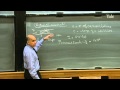
plus Qi now starting from here these two equations
and substituting this into this and then this back into this we can get the charge versus voltage relation first let
us take the depletion region QV relationship so we can write V is equal to minus QD by C plus SS
now we want QD as a function of v so to do that we must Express CS also as a function of
QD now if you recall when we wrote down the thr voltage expression okay we wrote down the
depression charge at threshold as follows QD is equal to minus of square < TK 2 Q Epsilon S NA a into
5T this was at inversion please look into the
derivation okay so basically this derivation is related to
this so we must relate this area QD and this electric field here and then this electric field is
related to the area under this which is the potential CS okay so following the same
approach if you try to derive the QD as a function of C all that we need
to do is replace 5 T by SS and here this is in general valid until
threshold okay which is in the depletion region so once you know this you know that SS
is given by QD s
by 2 Q Epsilon S NA by squaring both
sides so we can substitute this here and you will get an equation between V and QD so this is a quadratic equation so
your relation is V is equal to - QD by C plus plus QD ² by 2 Q Epsilon S
NA this is the equation for depletion region okay now how do you know
that this equation is valid well it depends on what is your value of Cs or V so depletion region means V less than or
equal to VT but greater than or equal to zero or SS is less than or equal to 5T
greater than or equal to zero let us write this here that is a
depletion now similarly let us take the inversion condition what is the charge voltage
relation under inversion now incident this uh quadratic equation represents this particular
curve okay please note how do we get this shape from
here the first term is a linear term okay and then the second term is a quadratic term basically subtracting
from the first term if you take the brackets so in Brackets if you write you can write this as
as follows so now this whole quantity will be on the negative axis
okay so a linear term increasing but then you have a quadratic term subtracting from the linear term so
that is what is seen here so you have a linear term a linear increase but then since the quadratic
term is there and subtracting the magnitude goes on falling and that is how you get this kind of shape
okay now let us return to the inversion charge so in inversion we can write V is equal
to QD inversion plus Qi with a negative sign upon C plus
5 T because inversion is characterized by V greater than or equal to VT or
SS equal to 5T so we must replace S by 5T which we can write as minus
Qi by C plus minus QD inverse inversion by C +
5T now this sum is nothing but threshold voltage VT
therefore you write this as V minus VT is equal to - Qi by C or
transforming this equation you get Qi is equal to minus C into V minus VT so you see Qi is linearly
increasing with voltage but please note this formula is only valid for V greater than
VT so one must not say that if V less than VT Qi will be positive there is no positive Qi for
V less than VT this formula itself is valid only for V greater than and VT okay in other words now you can see that
this particular shape is a straight line starting from VT okay that is a shape here that is the
shape for Qi so what we derive is that the inversion charge increases linearly with
the difference between the applied voltage and the threshold voltage now with this we have completed the QV
characteristics of an ideal MOS capacitor so let us summarize what we have obtained so
far so this is the Q versus V curve the various segments the equations are as follows for this accumulation
segment that is this segment here you can write
QA is equal to minus C into V that is this segment then for the depletion segment
that is between Z and VT you can write V is equal to minus QD by C
+ QD s by 2 Q Epsilon S NA now for this particular depletion charge segment Beyond threshold Beyond
threshold this value is minus QD inverse and what is this so QD is equal
to QD inverse which is nothing but minus of 2 Q Epsilon S NA a into 5T where 5
T is equal to 2 * VT long Na by n i then you have the inversion segment
that is this inversion charge segment and for this segment your equation
is Qi is equal to Min - c into vus VT the threshold voltage expression VT is given
by minus QD inverse by C which is oxide potential drop that
is squ < TK 2 Q Epsilon S NA a into 5 T upon C plus the Silicon drop that is 5T so these are the result for an ideal
MOS capacitor okay now we must see what happens
when the capacitor is not ideal or it is real now as we explained in a real capacitor the extra things that we must
take into account are firstly this metal or polysilicon gate and
semiconductor between them there is a contact potential which we have not taken into
account and also in addition you have a number of charges in oxide as well as at the
interface so the charges we listed where qit that is interface trapped charge q that is oxide trap
charge qf that is a charge at the interface fixed charge at the interface and qm that is a mobile charge
in oxide now we will not discuss the origin of all these
charges that is beyond the scope of our present work so we will concentrate on the
charge qf alone effect of qf now it turns out that
at silicon silicon dioxide interface you have a positive charge which is said to be fixed because the
value of this charge doesn't change with voltage it is always present whenever you create a silicon silicon dioxide
interface so right here at the interface you have this charge okay usually this charge is
shown in a box because because this is a fixed charge it cannot move nor can it vary with
voltage now very briefly the origin of this qf is as follows the chemical composition of the
oxide layer or silicon dioxide layer is S2 okay so this is Si O2 whereas this is Si now you cannot
have an Abrupt transition from SI to sio2 okay in practice so what is going to happen is that if you look at this
interface in detail so let us expand this interface so on this side you have
silicon and on this side you have silicon dioxide so there will be a region in which the composition will
gradually change from SI to S2 so here it is sio2 and this region it is sio X where X varies from
0 to 2 so here it is zero X is zero and here it is two so there is this
layer transition layer now because you do not have two oxide oxygen atoms for one
silicon okay so all the Silicon atoms are not satisfied by bonding and therefore there
is a charge that is created a positive charge that is created okay and this positive charge is the charge that is
called qf so in our non- ideal Mass capacitor which is the next topic that we will
discuss we will try to take into account the effect of qf
and what is called the contact potential or as we show that contact potential is nothing but work function difference
denoted 5ms this is called work function difference
now the question is how do we take both of these into account let us start with the effect of
qf what effect will qf have now you can see that this positive charge qf will tend to find negative
charge here okay in the nearest silicon
substrate so what does this mean this means that if you have a p type substrate here
then even when you don't apply any voltage because of this fixed charge you'll already have a depletion layer
so you have charge in Silicon even when there is no applied voltage recall that in ideal Moss
capacitor for no applied voltage there was no charge in Silicon whereas here you have a negative charge now if the qf
is very large you can even have inversion charge here in addition to depletion
charge so if you want to create the condition of zero charge in
Silicon what you'll have to do is you'll have to apply a voltage to the gate so that these
charges instead of terminating on this side with an electric field like this they
terminate on the gate with an electric field directed in the opposite way so you need electric field like this so
that this positive charges we will not look for negative charges in Silicon in other words you have to put a negative
charge equal in magnitude to the positive charge in the gate so which means you must apply a
negative voltage to the gate to create zero charge in
Silicon now zero charge in Silicon we said corresponds to flatband conditions in semiconductor if
the semiconductor is uniformly doped because then the conduction and balance bands are constant with
distance when there is no charge so therefore what we can say is that to create flatband conditions in
Silicon you will have to apply a voltage in a non-ideal moss capacitor and if you want to take into account only the
effect of qf then you will have to apply a flatband voltage which is negative and what is
the value of this flatband voltage that also we can determine since the charge is
qf okay the voltage to be applied from the field and charge picture is vfb is equal to
minus qf upon c not this is the simple Capa parallel plate capacitor relation that
is the charge is equal to voltage into capacitance okay so one can draw the charge and uh field picture here it
would be like this so you have fixed charge positive on the semiconductor and equal negative
charge on the gate so this is a charge condition both are sheet charges and now you have electric
field directed from this positive charge to negative charge so this is your E versus X and
the value of the electric field is nothing but qf upon Epsilon
Ox you recall that when we wrote the electric field in oxide because of a certain silicon charge Qs we wrote the
oxide field as minus Qs by Epsilon Ox so similarly here it is minus qf by Epsilon ox
qf is this charge area under this so now area under this is the applied
voltage so following this approach you get flatband voltage equal to minus qf by C so the effect of a fixed charge is
to shift the flatband voltage of an ideal Moss capacitor which is
zero to a negative value okay so the flatband voltage is shifted from zero to a negative value in a non- idial MOS
capacitor because of qf now how do you take into account the effect of
FMS to take into account effect of FMS we will have to go to the energy band diagram now this is an important point
that we arrive at here that whenever you want to discuss a
junction between dis similar materials okay then you will have to use the energy band diagram you cannot avoid the
energy band diagram if you recall when we discussed the PN Junction we said that when you have a PN
Junction made in Silicon that is in the same material one can do a great deal of analysis of this Junction and derive the
current voltage characteristics without the aid of energy band diagram although the energy
band diagram approach gives you some additional insights but with without energy band diagram one can go quite far
in understanding a p Junction which is a homo Junction okay so we can generally say to
understand a homo Junction we can avoid the use of energy bind diagram to a great extent but while understanding a
hetero Junction or a junction between dissimilar materials which is what a moss Junction is because material here
is different from the material here and of course the material here is also different okay so in such cases we need
to use the energy bind diagram to derive the effects of the contact potential or work function difference between the one
material and another material so next topic that we need to discuss in the context of non- adial moss capacitors is
the energy band diagram now let us look at the energy band diagram when all the components of the
MOs capacitor are isolated that means you have the metal then you have the
oxide and you have the semiconductor and suppose these are all isolated now uh without any loss of
generality we'll assume that the metal is also sufficiently thick this just to enable us to draw the
energy band diagram that is all now how do we draw the energy band diagram showing the bands in all the
three we must choose a reference we know that the reference is normally the vacuum
level so we first draw e the various steps in the drawing of energy band diagram were given in the
context of P injunctions We are following the same steps now in the metal
you cannot have conduction or bance bands you only have the form level so this is
EFM and this difference is normally referred to as the work function the difference between the vacuum level and
the from Level so this is Q * 5m where 5m is the work function in volts is energy
energy band in the oxide the oxide is an insulator it has a very wide band Gap so energy band diagram is something like
this this is the conduction and Valance band in fact you can show it even larger okay please uh remember that
these three are isolated right now when we draw the band diagram so there is no connection between in them so we are
drawing the structure individually in each of these three so this is
EC and this is EV now we come to the Semiconductor in the semiconductor you
will first locate the EC and then EV the band gap of semiconductor is
obviously much less than that of the oxide this EC is located at a distance given by Q * the electron
affinity then this EV is located below EC this is energy gap now since we are considering P type
silicon your firy level will be below the intrinsic level which is in the middle
here so this is intrinsic level so your for level is somewhere here so this is EF in the semiconductor s stands for
Semiconductor now here we have shown a metal whose work function is more than the electron affinity in the
semiconductor it is not necessary that this should always be the casee you can have the from Level Above This level
here or below even balance band level it depends on the metals in analogy to the work function
in metal you can define a work function in semiconductor
also so that would be this difference Q * 5 S although the the work function in
semiconductor doesn't have um that much real meaning as it has in a metal because you can remove an
electron from the form level out of a metal okay so when you remove a electron out of a metal it is most likely to be
at the form level whereas when you remove an electron in a semiconductor it is unlikely to be at
the form level because fir level is in the Forbidden Gap and you don't have any allowed states in the Forbidden gap for
but still it may help us in writing the equations that is why we are introducing
this work function in semiconductor so fir level in the metal is above the firm level in the
semiconductor as we have drawn here now from this starting point how do we proceed to the situation
when you put all this three components together and and join them by a wire so that means now we draw the band diagram
when it is like this so we are joining them together please note that just if you join them
together like this the band diagram will be no different from this diagram okay that is
because since there is an insulator here it prevents any interaction between the metal and the semiconductor so no
exchange of charges can happen so even when these three components are struck to each other they are still as isolated
as this case when they are separate so when we talk of the energy band diagram of a moss capacitor under
equilibrium it is necessary to note that the metal here is joined to the semiconductor here by a
wire only then the mass is said to be in equilibrium that is all these three form a system because in a system the various
parts should be able to interact with each other otherwise it is not a system at all
so in this case what is the energy band diagram we can start from here and we will note that since fromy level is
higher here than in this semiconductor the electrons will tend to be transferred in this direction so
electrons are transferred from metal to semiconductor now please note that electrons are being transferred from
metal to semiconductor because of from level in metal is higher than that in semiconductor one must not think that
because metals are in higher concentration uh the electrons are in higher concentration in metal than in
semiconductor therefore they are being transferred okay so many times students have this
means conception that because electrons concentration is higher in metal then in semiconductor always you
will have transfer of electrons from metal to semiconductor this is not correct for example here in this case if
the formy level was below this formy level here somewhere here like
this then even if this is a p type semiconductor which has a very small number of electrons when you join the
metal and semiconductor by a wire the electrons would get transferred from semiconductor to
metal okay because the from Level here is higher than here so it is a fir level difference that
decides because fir level represent the average energy of electrons and electrons always move from regions of
higher energy to regions of lower energy just as water goes from a point which is at a greater
height to a point which is at a lower height okay so even if you have a container like
this which is small and you have a big container
here at a lower height than this then when you join these two by a tube the water will flow from this to
this even though the container is small because it is at a greater height than here so it is a height that decides the
transfer of water similarly here it is the fromy level that decides the transfer of electrons direction of
transfer of electrons now how are the electrons transferred well even though the
electrons have been shown to be transferred like this it doesn't mean that they're going through the oxide
because the oxide would not allow any electrons so basically this transfer is taking place Through the Wire here so
this is how the electrons are transferred now after the transfer takes place and equilibrium is
established you know that both these form levels should be aligned because in equilibrium the form level should be a
constant therefore the band diagram would look something like this you should draw a constant from
your level now please note that we are not drawing a form level in
oxide because oxide is an insulator really speaking there is no form level okay having drawn the form level
now you identify a space chart region you are following the same sequence of steps which we followed for p
injunction now we ignore the width of the space charge region in the metal because that is really very
thin now here you see that if electrons are transferred here they would Rec combine with holes on the P
side and in effect what you are having is therefore depletion of holes so you are creating a depletion
layer therefore the extent of this region would be much more than a sheet charge because
you are having a depletion layer so whole concentration is going to decrease as compared to bulk now you
draw the energy band diagram in the bulk in the bulk it is bulk means away from the space charge
region so this is what is the energy B diagram in semiconductor away from the bulk and
now you must complete the picture the whole concentration is reducing as you come to the surface so it is something
like this okay and you can complete the picture for vacuum level this is e not
this is EC this is EV and this is EF so something like this is is your e not
now what about the vacuum level in the metal vacuum level in the metal will be at the same distance from the form level
as it was here now one way of understanding how this bending
occurs in energy band diagram is to build up this diagram as follows so here you find that the electrons will
move into the semiconductor and therefore the fromy level here will come down okay so we assume that the from
level is coming down here and it is trying to getting it is aligning with this
metal actually this is coming down and that is going up but for Simplicity we'll take this as the reference and
then we'll say this is coming down so along with this the E not also will come down so you have e not here somewhere
here so that is how the diagram looks note that we have not drawn the diagram in
the oxide you can draw it in the oxide also okay but that adds to the complexity and
for a first course we need not bother about this diagram in the oxide in fact whatever effects we are going to discuss
those effect depend on the energy band diagram in the oxide they depend only on the diagram in the metal and
semiconductor so this is the picture under equilibrium so you see what has happened is because of the contact
potential even when the applied voltage is zero you have a charge in the Semiconductor in this case it is a
negative charge so this is the effect of the contact potential that even when the applied voltage is zero you have a
charge in the semiconductor because of charge trans between metal and semiconductor originating from
difference in the from a levels in the two regions so that is the effect of non-
adality so which means if you want to create a zero charge condition in the semiconductor now you will have to apply
a voltage to the gate in other words the flatband voltage will not be zero that is the effect of the work function
difference now how much voltage should we apply so that the charge conditions are
zero when the charge when you have zero charge here the energy band diagram would be the same as this that is a flat
band condition okay
so to achieve this flat band condition you have to remove the negative charges which are there in P
type so from here we start and we have to remove the charges which are there in P type so to remove the charges
in negative charges in P type semiconductor you must apply a negative voltage to the metal so which means you
must lift this from level up because increasing energies here these are electronic
energies so when a from Level moves up it means that you are applying a negative
voltage so in order to get flatband condition what you will have to do is you'll have to introduce
a power supply here with a negative polarity because in this particular case you have negative charge
in the semiconductor so once you do that provided the power supplies of a proper magnitude we'll shortly see what the
magnitude is all these negative charges will be repelled so that is
interesting that you have zero charge condition in the metal for a given applied voltage so this is the flat bind
voltage now the difference in the fromy levels here so this is the condition now for V
equal to vfb so the band diagram for V equal to vfb is the same as the band diagram when
the three regions are isolated or not joined by a wire then this difference between the
form levels indicates the amount of Applied voltage because under equilibrium the form levels are Al
this is the flat blind voltage or the voltage you have to apply to the
gate now evidently this voltage is equal to the difference in the work function of the semiconductor and the metal okay
so we can therefore say that the effect of the work function depence FMS is that the flat bind voltage equal
to 5ms should be applied to create flatband conditions so we write vfb effect of 5ms is to create a
flatband voltage equal to 5ms 5ms is nothing but 5 m minus 5S okay so please note I repeat from here
that this voltage is equal to is the difference of these two okay but in magnitude it is negative so this voltage
is obtained as this minus this now the we have already seen that the effect
of qf was to create a flatband voltage equal to minus qf by
C so this was assuming that there was no FMS
so effect of qf when FMS is zero is this and effect of FMS when qf is zero so we considered no qf in this
case is this so whenever you want to understand the effect of two parameters you must understand them one at a time
that is what we are doing here okay so from these two we can easily get the effect of FMS and qf as
follows in presence of 5ms and qf you can simply write the FL bband
voltage is equal to the superposition of these two that is FS minus qf by C so we are
simply summing up these two to get the effect when both FMS and qf are present okay we can summarize all this
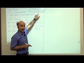
discussion on the effect of qf and FMS in a non- adal capacitor as follows this is the picture we had for the ideal
capacitor so zero charge condition in the Silicon at 0 volts and then Threshold at a voltage
given by this formula now the zero charge condition occurs at flatband voltage in other
words if you simply change this V to V minus vfb then this whole picture is valid same thing you do here also the
the charge was Zero for voltage equal to zero but now the charge is zero when voltage is equal
to vfb in other words if you change this to V minus vfb this whole diagram becomes valid and it becomes applicable
to a real capacitor so we can therefore say that the effect
of non idealities of qf and FMS is to Simply change the zero charge condition to Flat bind voltage and the threshold
voltage to the the following formula so the threshold voltage is now given by VT is equal to the threshold
corresponding to Ideal capacitor plus vfp right because V minus vfb is
this okay so therefore V is vfb plus this so VT of a real capacitor is VT of an ideal capacitor plus vfp we shall
continue the discussion in the next class [Music]
and
Heads up!
This summary and transcript were automatically generated using AI with the Free YouTube Transcript Summary Tool by LunaNotes.
Generate a summary for freeRelated Summaries
Understanding MOS Junction C-V Characteristics: Accumulation, Depletion, and Inversion
Explore the intricacies of MOS junction C-V characteristics and their operational regimes: accumulation, depletion, and inversion.
Understanding Conductors and Capacitors in Electric Circuits
Explore the critical concepts of conductors, capacitors, and electric circuits in this comprehensive guide.
Understanding Electric Potential, Fields, and Capacitors in Physics
Explore electric potential, fields, and the role of capacitors in energy storage.
MOSFET Large Signal and Small Signal Models: Analysis and Biasing
This lecture by Behzad Razavi explains the transition from large-signal to small-signal MOSFET models for amplifier design. It covers transconductance (GM) expressions, the importance of proper biasing, and how to use linear small-signal models for simplified analysis.
Understanding Circuits: Key Concepts and Theories
Explore the fundamentals of electrical circuits, current flow, and more with this in-depth guide.
Most Viewed Summaries

A Comprehensive Guide to Using Stable Diffusion Forge UI
Explore the Stable Diffusion Forge UI, customizable settings, models, and more to enhance your image generation experience.

Kolonyalismo at Imperyalismo: Ang Kasaysayan ng Pagsakop sa Pilipinas
Tuklasin ang kasaysayan ng kolonyalismo at imperyalismo sa Pilipinas sa pamamagitan ni Ferdinand Magellan.

Mastering Inpainting with Stable Diffusion: Fix Mistakes and Enhance Your Images
Learn to fix mistakes and enhance images with Stable Diffusion's inpainting features effectively.

Pamamaraan at Patakarang Kolonyal ng mga Espanyol sa Pilipinas
Tuklasin ang mga pamamaraan at patakaran ng mga Espanyol sa Pilipinas, at ang epekto nito sa mga Pilipino.

How to Install and Configure Forge: A New Stable Diffusion Web UI
Learn to install and configure the new Forge web UI for Stable Diffusion, with tips on models and settings.

If you found this summary useful, consider buying us a coffee. It would help us a lot!