MOSFET Large Signal and Small Signal Models: Analysis and Biasing
How to Analyze MOSFET Circuits: From Large Signal to Small Signal Models
This lecture provides a foundational understanding of MOSFET operation, distinguishing between large-signal (non-linear) and small-signal (linear) models. It explores the transconductance (GM) and its dependencies, solves a bias example, and demonstrates how to decompose a circuit into bias and signal components for simplified analysis.
Keywords: MOSFET transconductance, small signal model, large signal model, MOSFET biasing, circuit analysis, amplifier design, Behzad Razavi
Understanding MOSFET Transconductance (GM)
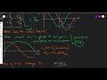
Transconductance (GM) is a measure of a MOSFET's strength as a voltage-to-current converter. It is defined as the slope of the ID vs. VGS curve. Three key expressions for GM are derived from the saturation current equation:
- GM = μnCox (W/L) (VGS - VTH)
- GM = 2ID / (VGS - VTH)
- GM = √(2 μnCox (W/L) ID)
Key Insights and Dependencies
The three expressions are all correct but represent different scenarios where one parameter is held constant:
- GM ∝ (W/L) if VGS - VTH is constant.
- GM ∝ (VGS - VTH) if W/L is constant.
- GM ∝ 1/(VGS - VTH) if ID is constant. This is possible by reducing W/L as VGS - VTH increases.
- GM ∝ ID if VGS - VTH is constant. This is achieved by increasing W/L.
Example: Placing two identical MOSFETs in parallel (W/L doubles) doubles the drain current and GM, provided VGS - VTH is constant.
The Necessity of Proper Biasing
A MOSFET requires a DC bias voltage (VGS) and a DC drain-source voltage (VDS) to operate in the saturation region for amplification. The circuit must:
- Provide a bias voltage (V0) between gate and source to establish a quiescent current (ID0).
- Ensure VDS > VGS - VTH to maintain saturation.
A simple resistor load (RL) cannot provide the necessary VDS. A DC power supply (V1) is needed to create a voltage drop across RL and set the correct VDS.
Example: For ID0 = 1mA, RL = 1kΩ, and VDSmin = 0.4V, the power supply V1 must be 1.4V.
Large Signal vs. Small Signal Operation
Large Signal Operation
This refers to the general case where the input signal amplitude is not assumed to be small. The complete, non-linear MOSFET model (ID = 1/2 μnCox (W/L) (VGS - VTH)2) must be used. Analysis can become complex, especially with multiple transistors. For a deeper understanding of the underlying physics, refer to Understanding MOS Junction C-V Characteristics: Accumulation, Depletion, and Inversion.
Small Signal Operation
When the input signal amplitude is small (Vmic << VGS - VTH), the circuit can be linearized. This allows superposition to separate the analysis into:
- Bias (DC) Analysis: Uses the large signal model to find DC voltages and currents.
- Small Signal Analysis: Uses a linear model where only time-varying components matter. DC sources are zeroed (voltage sources shorted, current sources opened).
The small signal model of a MOSFET is a voltage-controlled current source: id = gm * vgs, where gm is the transconductance at the bias point. This simplification makes circuit analysis much easier, similar to the analysis techniques used in Understanding Resonant Converters: Inverter and Rectifier Modeling Explained.
For an introduction to fundamental circuit concepts that underpin this analysis, see MCAT Physics Circuits: Current, Resistance, Capacitance & Measurement.
Greetings. Welcome to electronic circuits one. I am Behzad Razavi and this is lecture number 33.
Today, we will look at the MOS device again and this time we will delve into what we call large signal operation and
small signal operation and based on these two types of operation develop models for the for circuit
representation of transistors. But before we go there, let's take a look and see what we did last time.
In the last lecture, we went into one second order of second order effect in MOS devices, namely
channel length modulation. And we saw that as the drain voltage increases,
assuming that we are already in saturation, so we are over this hump here,
then what we see is that the pinch-off point actually gradually moves to the left towards the source.
And that means that the actual length of the channel decreases, which according to our equation
indicates that the current should increase. But rather than make L a voltage
dependent quantity and making things complicated, we simply multiply the original equation by this factor of 1
plus plus lambda VDS. So that when VDS goes up, the drain current also increases.
And that's a very simple representation that we use in many types of analysis and design.
All right. We also looked at the concept of biasing. We saw that if we have a MOS device and we just apply a signal to it
without anything else, the device is dead. There's no current in it. We are hoping that it will convert a
voltage to a current, but it doesn't do that if we just apply a little signal to, for example, a gate source
voltage, but nothing else. So we what we realized was that we have to apply a certain voltage between the
gate and the source even before a signal is applied to keep the transistor alive, so to
speak. We saw that if we apply a certain voltage, we have a certain current and that allows the drain current
to be a sharper function of the voltage than if you are over over here or if you are over here.
So in fact, this brought us to the concept of how much current change we get for a given voltage change and
that's what we might consider the strength of the device as a voltage to current converter.
So we actually defined the slope to be the transconductance of the device as a measure of its strength.
So what we expect is that if we bias the device at a higher voltage, higher VGS in the absence of the signal,
which means we also have a higher current, perhaps, then the transconductance is higher because this
is a non-linear equation, right? It's a non-linear equation. So because of this non-linearity, the
slope, because of the second order effect, this second the power of two, this slope keeps increasing as VGS
increases. And that tells us that a higher bias voltage for gate source gives us a higher current and a higher
slope. All right. So today, we will delve into GM a little more and try to understand
its properties. As I mentioned last time, we have three different expressions for GM. We simply take the
derivative of the current with respect to VGS. We take the derivative of this and the
first equation that we find is this. So GM
expressions. So we saw that if we take the derivative,
this two cancels this one half and then we just have mu n Cox W over L times VGS minus VTH. All right, so that's one
equation that we can use. mu n Cox W over L VGS minus VTH.
But there are other manipulations that we can perform to obtain other types of expressions. For example, I know here
that VGS if I divide both sides by VGS minus VTH
and multiply both sides by two, on this side I have two times ID over VGS minus VTH
and on this side I have mu n Cox W over L VGS minus VTH, which happens to be GM. So GM is also equal to two ID
over VGS minus VTH. Okay. And lastly, what I can do is
I can just remove this VGS substitute for this VGS minus VTH from this equation. So VGS minus VTH is equal to
this divided by this square root of that, right? So I replace this VGS minus VTH with that and that gives you
the third equation, which is two mu n Cox W over L times the bias current, the drain current.
Okay. Now, if you look at these carefully, something looks to be a little strange.
For example, here, GM is proportional to VGS minus VTH, whereas here, it is inversely
proportional to VGS minus VTH. Which one is correct? Well, both are correct, but it just depends on what we
are doing. So let's go back to this equation and understand that there are three
parameters under the designer's control that are related by this equation. W over L is one of parameters. VGS minus
VTH is the second one and ID is the third one. These three are related by this equation. Mu n Cox is a constant of
the technology. We don't have much control over that. So when we are looking at these
dependencies and we want to know how GM varies with this or this, we have to remember that
in addition to the overdrive voltage and in addition to W over L, there's a third parameter, ID.
Or in addition to ID and in addition to the overdrive voltage, there's a third parameter, W over L and so on.
So let me elaborate on this and see how what we mean exactly. Okay, so here, we can say that GM, for
example, is proportional to W over L if we keep VGS minus VTH constant.
So VGS minus VTH constant. All right, that's fine, no problem.
Or we can say GM is proportional to the overdrive voltage proportional to this if we keep W over L
constant. That's fine, too. Nothing exciting yet, right?
Okay. Now, let's go to this equation and see what it means. So again, we keep one of them constant. Let's say we keep ID
constant. So, if ID is constant, it means that I have biased the device
at a current of 1 mA, right? There's a 1 mA current in it before any signal comes in because I need a certain amount of
transconductance. Right? I need to be somewhere on the on the higher parts of the ID versus VGS
curve, right? I have to be somewhere around here. So, I need a certain bias current, ID0.
So, that's the amount that we're assuming here. Okay. So, if ID is constant, GM is
inversely proportional to the overdrive. So, GM is inversely proportional to the overdrive.
All right. So, here's the tricky part. This says that if the overdrive voltage increases,
GM decreases. Okay, provided that ID is constant.
So, now we have to ask ourselves, we are increasing the overdrive voltage, but ID is constant. Is that possible?
Is it possible to increase the overdrive voltage of a MOSFET, but keep its drain current constant?
Well, we go back here. Remember, there are three parameters here. So, is it possible to increase VGS
- VTH while ID is constant? Yes. We have to reduce W over L.
Is it possible? Yes, we can do that. So, this condition is possible. You just have to be careful
in terms of what it means. It means that if you are changing VGS - VTH in this experimentation,
and you'd like ID to be constant because we're trying to see the dependence of GM upon overdrive, then implicitly we're
assuming that W over L is decreased. All right. Okay. Now, let's consider the other case. Let's assume that the
overdrive is constant, but ID is changing. So, VGS - VTH
is constant, but and then that means GM is proportional to ID.
All right. What does this mean? So,
I would like to increase ID so that GM increases. That happens if I keep VGS - VTH
constant. But how can I keep VGS - VTH constant while ID increases?
All right. So, we just go back to that same equation. How can I keep VGS - VTH constant
while ID increases? Well, that implicitly assumes that W over L increases.
All right. So, this scenario assumes that the overdrive voltage is constant, meaning you connect the battery from
here to here. That's it. The constant battery, we don't touch it anymore. But then I'm trying to get a higher
transconductance by increasing the current. How is that possible? The only way
that's possible is by making the device wider. W has to increase or L has to decrease. So, W over L has to increase.
All right. And similar observations apply to this one. I just won't go there, but I want you to know
that these three are all valid. It just depends on what we're assuming constant and what's variable for each of these
scenarios. Okay. So, to drive this home, let's look at an example.
Uh we take a MOS device like this uh with a certain W over L.
All right. It has some mu and Cox, and it has some threshold. Now, we copy this device over here. So,
exactly the same type of device. So, here's another type of device. Another copy of the same device.
So, it has the same mu and Cox, the same threshold, and the same W over L. Doesn't have to, but we chose it to have
the same W over L. Now, I place these devices in parallel. And by that, I mean I connect the gates
together, I connect the sources together, and I connect the drains together.
All right. So, my question is, if
VGS is constant, which means VGS - VTH is constant, how does the GM
of the composite device compare with the GM of one device? So, let's think about that for a second.
We had one device with a dimension of W over L, and it had a certain battery between the
gate and the source. So, it had some current and it had some GM. We can calculate it
using any of these, right? Now, I came along and I added another device in parallel to this device. The
drains are shorted, the gates are shorted, the sources are shorted. In a sense, now
these two devices are equivalent to one device with
twice W. Okay? W over L here, W over L here, the result is 2W over L.
And you can actually see that if you look at the MOS structure, right? So, here's the MOS structure that we
have uh developed before in three dimensions,
approximately. So, this is W. I'm sorry, this is L, and this is W.
And I take another one, exactly the same, and I place these two in parallel.
So, now what happens is when these two gates are connected to each other, and this is also W,
we see that it is as if the two devices are connected like so, as if the W the width of the device has
doubled. Okay? Imagine you just take this and take this and place them next to each other. If you look at the top,
it might be more it might be clearer. So, from the top, this is what we have. Uh we have
these are the source and drains, or source and drain. This is the gate, and this is W, right?
From here to here is W. And then we have another one down here. Source and drain,
and this is also W. And now we just short these together, right? So, we short the sources
together, the drains together, the gates together. So, we just bring this closer and closer
to each other, these two merge, and we see that the total W is 2W. All right. So, what this tells us is
that we have two devices uh whose equivalent width is 2W. Now, if you don't like this visualization, no
problem. You can just write equations and see what happens, right? So, we have one current for this guy,
ID1. We have another current for this guy, ID2. And because the drains are connected and
the sources are connected, we have ID1 + ID2 for the overall composite device. And they have the same VGS because the
gates are shorted and the sources are shorted, right? So, I write ID1 is equal to ID2
is equal to 1/2 of mu n Cox W over L VGS - VTH squared. So, that means that the sum
ID1 + ID2 it's just two of these, right? So, it's
equal to 1/2 mu n Cox two times W over L VGS - VTH squared.
Realize that you realize that this two has to go here. It has nowhere else to go.
It cannot go to this voltage. We cannot take this two inside a square root because they have the same VGS.
This VGS is the same as before when I didn't have one device. And mu and Cox again is a constant of the technology.
It's the same for both of these devices. So, equivalently, if I want to put these two devices in a black box, the only
equivalency I can create is to say the new composite device is twice as wide twice as wide as each of these devices.
All right. Okay. So, now what happens to the transconductance of the device?
Well, we write GM. We can try to use any of these. The perhaps the simplest one is this one
because we kept VGS - VTH constant. Right? They have the same voltage. We just added one more device. So, GM,
which was 2 ID 1 over VGS - VTH.
This is the older GM. Old GM meaning one device. The new GM meaning both of these are in
a box. So, the new GM is
two times Now, we said that the current has doubled. So, 2 ID 1
divided by VGS - VTH. So, we see that the transconductance is doubled.
All right, so you you really have to be careful when we are considering various cases as to what is
kept constant and what is varied because then you get different results. So, here because VGS is the same for one device
or two devices, the overall GM is twice that of one of them. Uh but if you did something else, you
could get something else, right? For example, this equation says, if W goes up by a factor of two,
GM goes up by square root of two. All right, so you have resolved to have resolved all of these in your mind to
make sure there's no confusion. Very well. Let's uh go on
to the uh one other
uh question that I raised last time. I just want to make sure that uh you have the correct picture in mind.
So, let me go back to that example where we said, let's build an amplifier last time and I raised the question.
So, here's where we are. So, let's build
an amplifier. So, this is what we saw. We eventually uh had a MOSFET,
which is a voltage-dependent current source. We had a microphone. We had a battery.
And uh the battery gave us some bias voltage to make sure we have a certain
uh current and transconductance and all of that. And then we had a resistor because we
wanted the current coming out of the MOS device to be converted to a voltage. We usually like voltages as outputs and
maybe even inputs. So, we pass it through a resistor. And we said, this is our output voltage.
So, if the microphone signal uh is superimposed on a voltage, when the microphone signal changes, it
wiggles this current. This current changes. This current the changes current flows through this resistor.
This voltage changes and that's the amplified microphone signal. But then I mentioned that uh
we do need to make sure that the device is in saturation. In saturation, you have to have this
condition, right? So, the drain-source voltage cannot be arbitrarily small. It has to be greater than VGS - VTH. This
has to hold before the signal comes in and it has to hold even after the signal comes in. So, at least let's make sure
that is true before the signal comes in. All right, so when we have no signal, VGS is equal to V0.
Okay. So, that's some amount. Uh so, let's just give numbers here. So, let's say V0 is uh
I don't know, 0.9 V. And uh let's say VTH is 0.5 V.
Okay. So, what is the minimum amount of VDS that we can tolerate? This equation says it has to be 0.9 -
0.5. So, for this device to be in saturation, we require that VDS be greater than or equal to 0.4
V. All right, if VDS is less than that, we have a problem. We are in triode region,
not in saturation. Okay. Now, does this circuit allow or enable this device to be in saturation?
In other words, can we have this much VDS here? Well, so if we need this much VDS here,
um and there's a current flowing this way, where is that current coming from?
Uh this part is open. So, all of this current has to come from this resistor. So, we really are saying that a current
is circulating here. A DC current before the signal comes in without a source of energy, without a
battery. How could that be? It's not possible, right? If you think of this MOSFET just for a second as a resistor
between source and drain, you have a resistor here, we have a resistor here. That's it. We have nothing else. How
could we have a current? So, this circuit does not provide VDS of this much. In fact, there won't be any
current here at all. VDS will be zero. VDS will be zero. The device will be in triode region. Everything is dead.
Nothing Nothing good comes out of it. Okay, so we have a problem, right? And we need to figure out what to do.
All right, so I really want the VDS to be, for example, more than 0.4 V, right? With the numbers I have chosen.
Okay, so can I do this? If I want that, can I go ahead and uh do this? I will come along and I just
put a battery maybe right here. Put a battery between the source and drain and choose
that to be 0.4 V. So, now the battery guarantees that this voltage minus this voltage is 0.4 V.
So, it guarantees that the device is in saturation. So, is that a good idea?
I'll give you 90 seconds to think about it. Okay. So, what did you decide?
Can we use a battery like so to guarantee VDS equals 0.4 V? Well, yes, we could. The only problem is
that now we don't have an output signal anymore, even though we I am talking to the microphone.
Why? Well, you can see that if there's a battery here, by definition, the voltage
across the battery doesn't change. Right? That's the definition of a constant constant voltage source.
Which means the voltage across this resistor doesn't change with time. Which means this value is always 0.4 V.
If I speak into the microphone, if I speak loudly, if I speak softly, nothing comes out, right? This is always 0.4 V.
So, this battery in a sense has shorted out this resistor. Uh the resistor has no role in the
circuit anymore because uh this voltage is dominated by the voltage source.
So, that won't do. We have to think of something else. Okay, so we have to fix this situation
and uh let's draw the circuit again. Uh with all the stuff, we have a microphone,
a battery for VGS. And we still need this resistor.
The resistor is fundamentally necessary because the current coming out of the MOSFET has to go through a resistor to
create a voltage. Right? So, we need that resistor. All right, so uh
that resistor, let's draw it like this. Except that I will not connect the bottom of the resistor to here, to this
common rail. I will put a battery here. Another battery and we call this V1 for now.
So, now something interesting happens. Okay. All right, so let's hope that with the
addition of this battery, now we have a current flowing through the device, the transistor, and we have a reasonable
VDS, right? Let's hope something like this is happening. Okay, so VDS is from here to here.
And uh the question is, can I guarantee that this VDS is 0.4 V
while this resistor is still there and the current from the uh
MOS device is flowing through RL to generate some sort of voltage, which represents the amplified version of the
microphone signal? Okay, well, let's just give some numbers here just to
have something to work with. So, let's say this resistor is 1 kΩ. And let's say we are shooting for a bias
current of 1 mA here. So, we'll call this ID0 to indicate that this is the current
before the microphone signal comes in, when the microphone signal is 0 V. Okay.
All right. Now, how much is VDS in this case?
Well, 1 mA flows upward through RL, right? That's to go this way through the uh transistor.
So, it generates a voltage. 1 mA * 1 kΩ is 1 V, but that 1 V is like this, plus here,
minus here, cuz the current going is going upward. So, that's 1 V.
So, that would be RL * ID0, positive here, negative here. Okay, so let's write a quick KVL around
this loop to see what we get. All right, so we have VDS here.
Then we have, if I start from this terminal, I say minus VDS, minus V 1 V, which is RL * ID0, plus V1
= 0, right? That's my KVL. So, minus VDS, then I'm going this way, minus 1 V,
uh or this would be really minus ID0 RL, and then plus V1
= 0. I'm interested in VDS, so we see that VDS
is equal to V1 minus I will write ID0 RL, knowing that it's equal to 1 V right now, right? Minus 1 V. Uh
Okay, so this says that if we have, for example, 1 V of drop across the resistor,
and we need 0.4 V for VDS at least, that is not that hard. We just pick V1 to be how much? So, this should be 0.4 V,
and and this should be that we are subtracting 1 V,
right? So, that means that V1 has to be 1.4 V. Uh So, indeed, if I come in and add a
battery from here to here with a value of 1.4 V, assuming that we have 1 mA of current
and 1 kΩ resistance here, then the voltage that remains for this VDS will be 0.4 V,
and the transistor will be happy. All right, so this allows us to provide this proper biasing.
So, proper biasing of a MOSFET requires some sort of voltage between gate and source when there's no signal, and some
sort of voltage between drain and source, so that this condition is satisfied, right? For saturation.
That means that we need a battery here, and we need a battery here. So, as we will see later, we can try to
get rid of this battery, but this is eventually our power supply, right? It's an amplifier.
It's a it requires to draw some energy from a battery or something to amplify, and
that is the source of energy for this amplifier. All right, this answers that question,
and now we are ready to move on to the next topic. Okay, the next topic is a large signal
and small signal operation. And I want to talk about that. If you watched the bipolar videos, we talked
about these before, but I'm assuming you haven't, so we'll start uh looking at those concepts again.
All right, so large signal
operation. Well, uh we'll start with an example
just to get warmed up. So, here's an example. Uh suppose we have something very simple
like this. I have two batteries connected to the MOSFET, V1 here,
V2 here, or sorry, I I guess I'll call this V0 and V1. So, V0 and V1 just to be
consistent with the previous example. Okay, and I have this resistor
tied between the source and this point. Why? Uh just just for the heck of it. We're we're curious to see what happens.
All right, suppose that I have everything I need to know. I have W over L,
I have μnCox, uh threshold, everything else, and I would like to find the current that flows
through this MOS device. All right. Okay. So, here's the what we are trying to
find, ID. So, we have μnCox, W over L, μnCox, W over L, we have VTH, the
threshold of the device. These are properties of the device itself. Do we have VGS? No, we don't know this
gate-source voltage. Why? Well, because I know V0, but then there's a drop from here to here,
right? So, I don't know VGS yet. And I don't know ID yet. Okay, so I have to find ID
directly, or I have to find VGS and then find ID from this equation, assuming that the device is in saturation.
Okay, is that difficult? No, not really. I write a a KVL in this loop here. Uh if I have a current of ID in the
drain, that also ends up in the source. So, we have a current of ID here, right? So, that current is ID.
Which means the voltage drop across RS is equal to ID * RS. So, now let's let's write a KVL in this
loop here. We have this voltage, V0, is equal to
this VGS, VGS, gate-source voltage,
plus this voltage, which is ID * RS. Okay, very simple.
Now, we have two unknowns here, VGS and ID. Fortunately, there is a relationship
between VGS and ID elsewhere. Let's look. This one also gives us a relationship. So, we have two equations
and two unknowns, and we have to solve them. Right? So, let's move forward and see
what we can do. I will try to find VGS from here and plug it in here, because I'm trying to find ID.
So, let's try to find VGS from here. In fact, this is something good to know. VGS is equal to what?
We multiply by two, divide by μnCoxW over L, and then take the square root,
and then bring the threshold to the other side. So, we have 2 ID
over μnCoxW over L, and then plus VTH.
Okay, that's a good equation to remember. Previously, we always found ID in terms
of the overdrive. Now, we find VGS in terms of everything else. Okay. So, let's go ahead and plug that
in here, see what happens. So, that's equal to square root of 2 ID
divided by μnCoxW over L, plus VTH,
plus ID * RS. So, what we do know in this equation are
V0, the voltage we have applied here, and VTH, and μnCox, and W over L, and
RS. What we don't know is ID. So, we can find ID.
We can even find a closed-form equation for ID if we really want to. Uh what we would do is we take V0 to
that side, we take the square root to this side. Then we square both sides and simplify
and so on, we end up with a simple uh second-order equation that we can solve. Okay.
All right. The purpose of this exercise was to show you that because of this nonlinear relationship,
uh the calculations do get a little complex as we go along. Now, here it's not a big deal, because
we can find even a closed-form equation for ID. But
it's not always that easy. Uh let's suppose that I give you something like this. I have
one device like so.
And then I have another device like so. I connect the battery from here to here.
And stuff from here to here, another battery from here to here. Uh this is some voltage V0, this some other voltage
V0 prime. And then a battery from here to here, which is our usual
V1, right? Now this becomes substantially more complicated if you want to analyze it.
Because these two devices now interact here. We have some current from this guy, some current from this guy flowing
through this resistor. So it's a little messy. Okay, so things can become a little more
complex. All right. So far so good. I just calculated the bias conditions here,
right? I just found the current device. There was no signal yet. I used just how much current I might have. Could be a
milliamp, half a milliamp, 2 milliamps, some amount. All right. Now let's go ahead and apply
a signal on top of this bias that we have. After all, we're trying to build an amplifier. So a signal should be
coming in and we're curious to see what the signal does. So let's go ahead and add a signal
and see what happens. So let's add
a signal. So here's the situation. I add microphone signal here. I have the
original mic original battery of V0. This goes to the gate source of the MOSFET.
And then for now we just have a battery here. Don't worry about anything else. So we call this V1,
V0. This generates a signal Vmic
uh from here to here. And then we have a certain current here ID.
So we're just interested in the drain current for now. Remember that eventually this current has to flow
through a resistor, all sorts of things. But for now we're considering a very simple case.
Okay. So let's imagine that Vmic is just a simple sinusoid. So Vmic
is equal to VM sine of omega t.
That's all. It's a little sinusoid with zero DC. It just goes up and down around zero, right?
Okay. Uh but it's added to V0. So this VGS now has V0 plus this in it, right?
Okay. So can I find ID? Well, I have the same equation as before except that V0 is replaced with V0 plus Vmic.
So I can say V0 plus Vmic or actually I'll just write the equation for it.
V0 plus VM sine of omega t is equal to
uh what did we have there? We had square root of 2 ID over mu n c ox w over l plus the
threshold voltage and then plus ID times RS. Okay, so we simply replace V0 with V0
plus the signal from the microphone. Okay, I'm still trying to find ID. Can I find ID here? Yes, we can find ID.
Uh again, we have to take all of this to this side and this square root to this side. Then we have to
square both sides. We end up with a quadratic equation. We solve the quadratic. We end up with some complex
square roots and things in there for ID in terms of all of this. So this will go under square root and all sorts of
things. It'll be a little messy. All right. So this is what we call large signal
operation. Why? Because I never mentioned whether this VM small or not. So in the general
case it might be large. So we say large signal
operation if VM
is not small. Now we don't know what small means.
Small with respect to what? But that's okay. For now just assume it's not small.
So by large signal operation we mean the signal that's coming to the circuit has a certain amplitude
and that amplitude is not assumed to be small enough. Small enough for what? We'll have to
see. But it's not assumed to be small. So it can be anything you want, right? It can become very large. It can be this
VM can be 10 millivolts, 15 millivolts, 100 millivolts. We haven't specified anything.
If you haven't specified anything, we continue to use the complete model of the MOS device.
Which is ID is equal to 1/2 of mu n c ox w over l times VGS minus VTH squared. Now if you want to include channel
length modulation, then well, times 1 plus lambda VDS. All right. So uh by large signal
operation, that's what we mean. The signal is coming in. We don't have any particular limit on it.
Uh a common mistake by students is that they say large signal operation means DC calculations.
That is not correct. They say bias calculations. That is not correct. It happens that for bias calculations we
use the large signal model, but it doesn't necessarily mean all the time that large signal means just bias.
So if we have large signal operation, we use the complete model, which we call the large signal model.
So we say use large signal
model of the transistors.
So what was the model of the transistor? Do you remember from last time? Well, we said that we have a gate.
We have a source. Not much going on between gate and source, so that's sort of open.
We have VGS. And then we have the current source here.
After all, it's a voltage dependent current source. And then here we had 1/2 of mu n c ox w over l VGS
minus VTH squared. This is the drain. And if you want to include channel length
modulation, then 1 plus lambda VDS. So if we don't have any restriction on the signal amplitude coming in, then we
have to use this model, which we call the large signal model. All right?
Okay, very good. Now as I said, once we have a few transistors or more, things can get pretty complicated.
Right? Because there each of these has this type of model and then we have various devices, various currents,
various voltages. We end up with some number of equations, a number of unknowns, and then many of these
equations are non-linear. So the calculations can get messy. All right. Now under some conditions
we can simplify the situation. Okay, so we have to see what those what those conditions are. And those are what
we call small signal operation. So let's uh talk about small signal operation and see what that means.
Small signal operation.
So as the name implies, we are hoping that in some cases the signal that's coming in, the microphone signal,
whatever it is, has a small amplitude. Again, how small is small? We have to see. But it's small.
So let's see. If the signal amplitude is small, is there any simplification that we can apply to our models and circuits,
etc., so that we can quickly find the properties of the circuit? Okay. So again, we start with an
example. So here's what we have. We have a microphone as usual
and the battery as usual. And again, I've just simplified everything, so we just have another
battery here. V1, V0, Vmic.
And in fact, this time I don't even have uh I'm sorry, there was a resistor here I
forgot to draw RS. But this time I don't have a resistor, so no RS here.
Okay. So um again, I know that this drain current
is related to this VGS. And it just happens that now VGS is equal to the microphone signal
plus V0. If you remember that was not the case here, right? VGS was not equal to this
because of the drop across the resistor, this term here. But here, it's very simple.
VGS is just equal to this. So, I can write ID directly. I can write ID
is equal to 1/2 of μn Cox
W over L VGS - VTH
squared. Um so, by the way, lambda is zero as usual, and VGS has a known value. VGS is
the microphone signal plus V0. And the microphone signal again we assume to be Vm sin of omega t, right?
Okay, so that's equal to 1/2 of μn Cox W over L I will group these a little.
So, I will write this as VGS - VTH plus uh Vm sin of omega t
squared. Now, if Vm is not small, this is it. That's how we calculate ID. No question
about it. But if I if Vm is small, maybe we can make some simplifications.
All right. So, if Vm is small, what's our first reaction here? Well, maybe I can factor out VGS - VTH
to get one plus a small number, and then expand that using a simple approximation.
Okay, so we will write this. So, we say, "Assume Vm
is much less than VGS - VTH." And that tells us now what we mean by small.
Okay, so then ID is equal to uh let me actually
write this down here because I need more room. So, ID
is equal to 1/2 of μn Cox
W over L All right. So, I will factor VGS - VTH out of here.
So, what I get is VGS - VTH squared. So, VGS - VTH
squared. And then what remains inside here is one plus Vm sin of omega mt omega t divided
by VGS - VTH. One plus Vm sin of omega t divided by VGS - VTH.
Now, because this term is much less than one I can write I can exploit this. One plus
epsilon to the power of two is approximately equal to one plus two epsilon, right?
So, let's write it like that. So, we have one plus two times Vm
sin of omega t divided by VGS - VTH. So, the key is that because this term
over this over this is much less than one, we managed to go away from this non-linear behavior and represent the
result by this simple linear expression. Okay, so let's examine this closely and see whether we can make make any sense
out of this. All right. Okay, so what is this? Do we know what
this means, what this is here? Uh given that uh VGS Okay, sorry. Let me go back here and
make a small correction. I'll do it in a different color so that you remember what happened here.
So, here uh what we really have for VGS is V0 plus V microphone, right? So, this
should be V0. And this should be V0. And then this should be V0.
And then this should be V0. Okay, the battery, the bias value that we have for the gate source before the
microphone signal comes in. Okay, so do we recognize this whole thing here?
Is the is a current quantity, right? And it's a current quantity given by this battery.
So, that would be the bias current of the device, which we usually call ID0. So, this is ID0.
Just the bias current. So, let's uh write this and see what we get. So, we have ID
is equal to ID0 plus two
ID0 over V0 - VTH times Vm sin of
omega t. So, now that's not surprising. What we got is the following.
The total current that flows through the transistor, ID, is equal to the bias current. Of course, we have bias
current. Plus the signal current. The signal current is the perturbation created in the current when the signal
comes in and go as applied to the gate source, right? So, we might call this the bias current.
And we might call this the signal current. You can see that if there's no signal
if Vm zero, there's no signal current, right? That's the perturbation that we have created inside this device here
when the microphone signal goes up and down. Okay, that's very interesting. So, that
uh suggests something. Maybe when I'm considering this MOSFET here with all the things that are going
on I can in my mind separate it into two separate circuits, two independent
circuits. All right. So, here's what we will do. We take that circuit. So, let me draw it
quickly again here. Uh sorry. Let me do that with the microphone first.
So, we have a microphone. Then we have a battery. And then we have this.
And what we see is that when I'm talking to the microphone uh V0 V1
then I get this total ID here, right? So, I'm thinking maybe I can decompose this into two.
Here's one. I have a MOS device with no signal coming in, just the bias quantities.
So, here's the MOS device with just the bias quantities. So, we have V0 V1, a certain
current ID0. This scenario takes care of this current here.
All right. And then on top of this superimposed on this, I have another circuit which is like this.
It's taking the microphone signal and generating a certain amount of current, which is all of that stuff
there. Two ID0 over VGS uh sorry, V0 - VTH times Vm sin of omega t.
So, in other words, what I'm really trying to do is this. I'm saying that this device
consists of really two currents. One current is constant and equal to ID0.
That's the bias current. And then superimposed on that, we have another current that's flowing, and that current
is this guy here. So, two ID0 over VGS - VTH times Vm
sin of omega t. Okay. And uh what we what's going on here is
we have a microphone signal. And then we have a battery. Uh this represents what we have so far
here. All right. Now,
uh it's a little strange, uh but I guess I would need to draw this battery as well just to have a complete
situation. And that's okay. We'll draw that, too, V1.
And that's the overall picture, right? Between the gate and the source, we don't have any impedance because the
current drawn by the gate is very small. So, but we still have a voltage here, right? That's the VGS that we have
that's total VGS that we have. Okay. All right.
So, uh one interesting observation What is this this uh factor here? Is it
familiar? This factor is the following. It's a bias quantity because there's no signal
in it, right? And it's equal to twice the bias current divided by
the bias overdrive voltage. Because V0 is here.
And when there's no signal, the gate source is equal to V0. So, it's like V VGS under bias
conditions minus a threshold. So, that's the overdrive voltage under bias conditions.
So, this is entirely bias dependent. It's not single signal dependent, hopefully. So, and it looks familiar.
Twice the drain current divided by the overdrive. What is that? Well, if we rewind
and look what we obtained before, we see that it is the transconductance of the device.
That's not surprising. The transconductance device says, "If you give me a voltage change of
delta V between the gate and source, I will give you a current change equal to GM times delta V."
Right? That is the definition of transconductance. So, if we go back here, you can see
if you give me a change in VGS, then I give you a change in the current equal to GM times the change in VGS.
So, the microphone signal is creating a change in VGS. And as a result, we get a change in the
drain current, and these are related by GM. So, it's not surprising that what we have here is just a transconduct-
transconductance of the device times the voltage that we applied. So, this is GM
times VM sin of omega t. Okay, so the pen is sick again. All right, so sin of
Let's see. sin of omega t. All right, so let's take a step back and
see what happened here. We have a bias voltage between gate and source. That gave us a certain bias
current. Because device is presum- is presumably in saturation.
All right, then on top of that we came in with a signal. We had a signal voltage that was applied
to the gate source on top of that bias voltage, right? So, signal voltage on top of the bias voltage.
So, this signal voltage changed this VGS. And that change got multiplied by GM to
give us a change in the current. And that's what happened. We had the voltage multiplied by GM, and that gave
us a change in the current. This current represents the change in the bias current. This is the bias current. This
is the change in the current. This bias current is just from bias conditions. This is from signal conditions. So, we
can look at this as the change in the bias current. All right, so maybe what we can do is we
decompose this according to this picture, and we say, "Here's one picture where we have
V0 and we have a current. And we have a voltage here, V1.
And this current is given by 1/2 of μn Cox W over L uh V0 - VTH squared.
All right. Okay. And then so, this took care of this voltage, this current, and this
voltage because they are all bias quantities, and they do not change with time.
Now, next to this, we draw another circuit for this guy. What is that? Okay, that has a voltage
coming from the microphone. So, we draw the voltage for the microphone,
V mic. And then we go to another current source,
which is equal to GM times the input voltage, the microphone
voltage, right? So, GM V mic. Okay. Uh this is the same as V mic. And then
what happens to this point here? Well, this point comes back here because I am using superposition.
I'm saying that uh this circuit plus this circuit should give me this circuit.
Right? So, uh if I have a V voltage of V1 between drain and source, I have to have it only
in one of these two models. I cannot have it in both models. So, this is what we call the large
signal model, if you will, which also used for bias calculations. And this is what we call the small signal model.
Small signal model of the MOS device.
So, it's very important to understand that small signal operation means the signal that's coming in
creates a very small change in everything. In particular, it's creates a small change in the overdrive voltage
because that was our condition. Right? The overdrive voltage is changed negligibly as a result of this. You can
see here that uh this term is much less than this term, so the overdrive voltage is not affected much by the voltage
that's coming by the signal voltage. All right. Alternatively, we can say that the signal creates small changes in
the drain current. So, we have a bias current of, let's say, 1 mA.
And then we have some small changes around that. These could be maybe 0.1 mA or something 0.1 mA or something like
that. So, that's called small signal operation.
And then in that situation, and only in that situation, can we simplify the circuit to a bias model and a signal
model. And the signal model, the small signal model, consists of something that represents only changes
in the current or voltage. We look at anything that is changing with time.
The microphone signal changing with time has to be there. The There's a component in the current
of the device that's changing with time. That has to be there, too. But everything that doesn't change with
time, everything whose change with time is zero, is zero here. Is zeroed out.
So, this voltage doesn't change with time. Its change with time is zero. Because we
are looking for only time varying components, it's not here anymore. You see, it's not in series with this.
This voltage represents a constant value. Its change with time is zero. Because its change with time is zero, it
has zero value here in the in this small circuit. So, this is what we call the small
signal model. You can see that small signal model now easily lends itself to linear
calculations. We don't have any uh in terms of the signal itself, it's just a linear model. We don't have any square
or anything else, so it's much easier to handle. All right. Our time is up. I will see
you next time.
The three key expressions are: GM = μnCox (W/L)(VGS - VTH), GM = 2ID / (VGS - VTH), and GM = √(2 μnCox (W/L) ID). Each expression is useful depending on which parameter is held constant, such as device dimensions (W/L), overdrive voltage (VGS - VTH), or drain current (ID).
Transconductance (GM) measures how effectively a MOSFET converts a voltage change at the gate into a current change at the drain. It is defined as the slope of the drain current (ID) versus gate-source voltage (VGS) curve. GM is crucial because it determines the gain of the MOSFET amplifier, with higher GM values leading to better amplification.
GM is proportional to (W/L) when overdrive voltage (VGS - VTH) is constant, and proportional to (VGS - VTH) when W/L is constant. However, when drain current (ID) is constant, GM is inversely proportional to (VGS - VTH). To increase GM while keeping ID constant, you must reduce the overdrive voltage and increase W/L.
Proper biasing sets a DC gate-source voltage (VGS) and drain-source voltage (VDS) to keep the MOSFET in saturation, enabling linear amplification. A simple resistor load alone cannot provide the required VDS; a DC power supply is necessary to create the correct voltage drop and maintain VDS > VGS - VTH.
The large-signal model uses the non-linear square-law equation (ID = 1/2 μnCox (W/L)(VGS - VTH)²) for large input amplitudes. The small-signal model linearizes this behavior when the signal is small, representing the MOSFET as a voltage-controlled current source (id = gm * vgs), which simplifies analysis using superposition.
First, perform a DC bias analysis using the large-signal model to find the operating point and transconductance (gm). Then, build the small-signal equivalent circuit by zeroing all DC sources (shorting voltage sources, opening current sources) and replacing the MOSFET with the small-signal model. Finally, solve for the time-varying voltages and currents.
Placing two identical MOSFETs in parallel effectively doubles the width (W/L), which doubles both the drain current (ID) and the transconductance (GM), provided the overdrive voltage (VGS - VTH) remains constant. This technique increases the amplifier's strength without changing the fabrication process.
Keep this summary
Save it to LunaNotes and it becomes a real note in your library — editable, searchable, and ready to turn into flashcards or a diagram. Free to start.
Save to LunaNotesOr summarise for another video.


32K+ people have turned 65K+ videos into notes
“Very useful tool. I'm using it for the last couple weeks and I'm loving it so far. Makes learning on YouTube a great experience.”
 Bhai Chrome Web Store review
This summary and transcript were automatically generated using AI with the Free YouTube transcript summary tool by LunaNotes.
Related summaries
Understanding MOS Junction C-V Characteristics: Accumulation, Depletion, and Inversion
Explore the intricacies of MOS junction C-V characteristics and their operational regimes: accumulation, depletion, and inversion.
Understanding Metal Oxide Semiconductor Capacitance and Voltage Characteristics
Explore the intricate details of MOS capacitors, their voltage characteristics, and implications of non-ideality.
Op-Amp Imperfections: DC Offsets, Bias Currents & Speed Limits
Explore the non-ideal behavior of operational amplifiers in this final lecture of the Electronic Circuits 1 series. Learn how DC offsets cause integrators to saturate, how input bias currents introduce errors in amplifiers, and how finite speed and slew rate limit op-amp performance.
Understanding Circuits: Key Concepts and Theories
Explore the fundamentals of electrical circuits, current flow, and more with this in-depth guide.
Understanding Resonant Converters: Inverter and Rectifier Modeling Explained
This video provides a detailed exploration of resonant converters, focusing on their construction, operation, and modeling. Key topics include the role of inverters, resonant networks, and rectifiers, with an emphasis on first harmonic approximation and the distinction between current-driven and voltage-driven rectifiers for efficient DC-DC conversion.
Most viewed summaries

A Comprehensive Guide to Using Stable Diffusion Forge UI
Explore the Stable Diffusion Forge UI, customizable settings, models, and more to enhance your image generation experience.

Kolonyalismo at Imperyalismo: Ang Kasaysayan ng Pagsakop sa Pilipinas
Tuklasin ang kasaysayan ng kolonyalismo at imperyalismo sa Pilipinas sa pamamagitan ni Ferdinand Magellan.

Mastering Inpainting with Stable Diffusion: Fix Mistakes and Enhance Your Images
Learn to fix mistakes and enhance images with Stable Diffusion's inpainting features effectively.

Pamamaraan at Patakarang Kolonyal ng mga Espanyol sa Pilipinas
Tuklasin ang mga pamamaraan at patakaran ng mga Espanyol sa Pilipinas, at ang epekto nito sa mga Pilipino.

How to Install and Configure Forge: A New Stable Diffusion Web UI
Learn to install and configure the new Forge web UI for Stable Diffusion, with tips on models and settings.
Found this summary useful?
Take it with you. One click puts it in your own LunaNotes library.
Save to LunaNotes