Comprehensive Guide to Zener Diode Operation and Voltage Regulation
Introduction to Zener Diode
- Zener diode is a special diode widely used for voltage regulation to maintain a constant voltage across varying loads.
- When reverse biased, it can be modeled as a constant voltage source equal to its Zener voltage (VZ), specified in its datasheet.
Application in Voltage Regulation
- Connect the Zener diode in reverse bias across a varying load (RL) to maintain a stable voltage.
- The diode allows varying current while keeping voltage constant, making it ideal for voltage regulation.
Breakdown Mechanisms
Avalanche Breakdown
- Occurs in lightly doped (normal) diodes under high reverse bias.
- Electrons gain kinetic energy, break covalent bonds, and cause a chain reaction producing large current.
Zener Breakdown
- Occurs in highly doped Zener diodes at lower reverse voltages.
- Breakdown is due to direct rupture of covalent bonds caused by a strong electric field at the junction.
- Zener breakdown happens earlier than avalanche breakdown due to increased doping.
Power Dissipation and Biasing
- Zener diodes have higher power dissipation capabilities than normal diodes, allowing operation in breakdown without damage.
- In forward bias, Zener diodes behave like normal diodes with similar characteristics.
- Important: Zener diodes can be used in both forward and reverse bias regions.
Symbol and Equivalent Circuit Models
Symbol
- Similar to normal diode symbol but with a bent line on the cathode side representing the Zener diode.
Forward Bias Equivalent Model
- Modeled as a barrier potential (~0.7V for silicon) in series with a small diode resistance (RZ).
Reverse Bias Equivalent Model
- Before breakdown: acts like an open circuit with very high resistance.
- At breakdown: modeled as a voltage source VZKN (Zener knee voltage) in series with resistance RZ.
- If RZ is negligible, the model simplifies to a constant voltage source VZKN.
Key Parameters
- VZKN: Knee voltage where breakdown starts, found in datasheets.
- RZ: Dynamic resistance of the diode in breakdown region, calculated as the inverse slope of the VI curve.
- Power dissipation rating: Maximum power the diode can safely dissipate, critical for design.
Depletion Layer Comparison
- Normal diode has a wider depletion layer.
- Zener diode has a narrower depletion layer due to heavy doping, enabling earlier breakdown.
Summary and Practical Use
- To use a Zener diode as a voltage regulator, connect the N side to positive and P side to negative terminal (reverse bias).
- Use the simplified equivalent model (constant voltage source) for most numerical and practical applications.
- Always consider VZ and power dissipation ratings from datasheets before implementation.
This comprehensive understanding of Zener diodes equips you to effectively use them in voltage regulation circuits and analyze their behavior under different biasing conditions.
For further reading on related topics, check out:
- Understanding MOS Junction C-V Characteristics: Accumulation, Depletion, and Inversion
- Understanding Metal Oxide Semiconductor Capacitance and Voltage Characteristics
- Understanding Inductors in Circuit Theory: A Deep Dive
- Understanding Circuits: Key Concepts and Theories
- Understanding Conductors and Capacitors in Electric Circuits
in this lecture I will introduce Xena diode Xena diode is a special diode and it is widely used in voltage regulation
to maintain a constant voltage across a varying load it is widely used in voltage regulation if we want a constant
voltage across a varing load we use xener diode for this purpose let's say RL is the ver load RL is the varying
load I will connect Xeno diode like this this is the symbol of xener diode and if this xener diode is reverse biased if
this xener diode is reverse biased then we can replace the Xena diode we can replace the Xena
diode by a constant voltage source and the voltage is equal to VZ and this voltage is given in the specific sheet
of the xener diode we have different voltages for different xener diode this is the varying load RL and we can have
the varying current with constant voltage so the xener diode is used for voltage regulation before moving to the
equivalent circuits of Xena diode I will explain two types of breakdown the first one is Avalanche breakdown the second
one is xener breakdown in case of avalanche breakdown we apply a high reverse Bas potential across the diode
the electrons gain High kinetic energy and break the calent bond and they also free more electrons due to the
collisions and we have a chain reaction and because of this large current is produced the avalanch breakdown occurs
in lightly doped diodes lightly doped diodes lightly doped diodes are
the normal diodes normal diodes Xena diodes are highly dope diodes and in case of lightly dope
diodes when you apply High reverse bass potential the electrons will gain the kinetic energy and they'll break the
calent bond and collide with other electrons this process will free more electrons and we have a chain reaction
and because of this large current is produced but in case of xener breakdown we can achieve the breakdown much
earlier let me write this down breakdown break down is
achieved is achieved much earlier much earlier in case of xener diode and
this is because we increase the doping level on both the sides on N side and P side we increase the doping levels and
we have the breakdown earlier as compared to the normal diodes in case of xener breakdown breakdown is initiated
by direct rupture of covalent bonds by direct rupture of covalent bonds by direct rupture of calent bonds I mean
tearing of covalent bonds this means steering steering of calent bonds and this happens due to strong electric
field at the junction developed by high reverse bias potential so there is difference between Avalanche breakdown
and xener break down in case of avalanche breakdown electrons gain the high kinetic energy and they break the
calent bonds on the other hand in case of xener breakdown there is direct rupture of covalent bonds because of
high electric field I hope Avalanche and zener breakdowns are now clear to you now we will move to the next point the
power dissipation capability Zena diodes are special diodes whose power dissipation capabilities are much more
than the normal diode and because of this they can easily work in Breakdown reason so xener diodes have high power
dissipation capabilities as compared to the normal diodes when we use the normal diode in Reverse Bas condition their
properties will degrade but on the other hand if we use the zener diode in Reverse bass condition the properties
will not degrade Zena diode in forward bias reason is similar to the normal diode in forward bias reason so this is
very important point because most of the people relate Zena diode to the reverse bias condition only but xener diode can
easily be used in forward bias reason also there is no difference between the zener diode and normal diode in case of
forward bias reason we can also use Zer diode in forward bias reason it will have similar characteristics as normal
diode this is one important point the most important use of xener diode is voltage regulation and xener
diode acts as voltage regulator when we operate it in reverse bias reason but we can easily operate zener diode as normal
diodes in forward bias reason now we will move to the next point that is the symbol of xener diode the
symbol of xener diode first we have to make the symbol of normal diode this is the symbol of
normal diode P side n side and after this I will make crooked n The Crooked n like this and this is the symbol of
xener diode the voltage is represented by v subscript Z this is the xener voltage now I will try to obtain the
equivalent models for xener diode using the vi characteristics of xener diode this is the forward bias reason and this
is the reverse bias reason in case of forward bias reason I have already explained the xener diode is similar to
the normal diode this is the symbol of xener diode I will connect P side to the positive terminal and N side
to the negative terminal now the xener diode is forward biased and I can replace this symbol I can replace this
symbol by the barrier potential 0.7 Volts for silicon and the diode resistance the diode resistance r z this
is positive negative and if we consider RZ to be very small we can have the equivalent
model like this in case of forward bias reason very simple now we will move to the reverse bias reason and I will
consider this reason from here to here and this is the reason when there is no breakdown this is the reason before the
breakdown and in this reason all also the xener diode will act as the normal diode and I will try to obtain the
equivalent model this is plus this is minus because we have to reverse bias the diode n side is connected to the
positive terminal and the P side is connected to the negative terminal and when this happens the current through
the diode is very small and when current is very small we replace the diode with high resistance
and we can consider it as open circuit so this is the equivalent model for the reason before the breakdown now we will
move to the most important part of this lecture we will try to obtain the equivalent model of the xener diode when
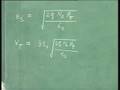
there is breakdown this voltage is VZ K vzk is the voltage after which the breakdown occurs then we have another
voltage VZ KN we can obtain VZ KN if we extend if we extend this linear reason this will cut the voltage axis at this
point and this voltage is VZ KN and let's take a random point on this linear reason and the corresponding current the
corresponding current is i z the corresponding voltage the corresponding voltage is v z and this current here is
i z k this is the knee current now we have everything to obtain the equivalent model of xener diode in
this reason I will first draw the symbol we have to reverse bias the diode so I will connect this side to the
positive terminal and this side to the negative terminal then we have the potential
v z KN + minus and then we have the resistance of diode RZ and this is equal to this is equal to v z VZ is simply
equal to VZ KN VZ KN plus this voltage and this voltage is equal to this voltage is equal to RZ multiplied by i z
the resistance of the zena diode and the current flowing through the DI so we have VZ KN plus i z r z and if you
want to calculate the value of RZ then it is equal to 1 by slope of the curve and we can easily obtain the zener
voltage if we have this values if we consider RZ to be very small if we consider RZ to be very small then we
have the model like this plus minus VZ kn and this is v
z so VZ is equal to VZ KN if we neglect the diode resistance r z and this is the equivalent model of the zener diode and
this is very important here you can clearly see this is VZ KN here you can clearly see the zener voltage is equal
to VZ KN and VZ KN is already mentioned in the specification sheet so if you need five volts or six volt PS of
constant voltage across any resistance then you can easily connect the zener diode across the resistance and if we
apply reverse bias potential across this diode we have 5 volts or six volts across the resistance because you can
see VZ is equal to VZ KN a constant voltage and we can say that the xener diode is acting as a voltage regulator
VZ and power dissipation is mentioned in the data sheet they are mentioned in the data sheet and these two values are the
most important values and you must have to consider them before any use and if we draw if we
draw the diagram for normal diode and xener diode then you can see the difference in the depletion layer this
is the depletion layer of normal diode this is p side this is n side and this is the depletion layer and in case of
xener diode in case of xener diode the depletion layer is much narrow this is the depletion layer this is the
depletion layer in case of zener diode and this depletion layer is narrow if you compare the depletion layer in case
of normal diode I will quickly revise the equivalent model of xener diode first thing we have to do is to connect
the N side of the diode the N side of the diode to the positive terminal and the P side of the diode to the negative
terminal so that the diode is reverse biased and once the diode is reverse biased we have the equivalent model like
this this voltage is VZ KN r z is the resistance and if you neglect r r z if we neglect RZ then we
only have we only have VZ KN as the value of xer voltage in this case VZ is equal to VZ KN plus the current is i
z i z RZ this is the value of VZ in this symbol also I will represent the current i z this is the
direction of the current i z because this is the reverse bias current and in this case when we neglect the
RZ VZ is simply equal to VZ KN in numerical problems we are going to use this model this model is mostly used we
neglect RZ and we have VZ not as the value of VZ this is very important model because in most of the numerical
problems you have to use this so it is better if you draw this model somewhere and you must also know how to obtain the
models using the vi characteristics this is all for this lecture see you in the next one
A Zener diode is a special type of diode designed for voltage regulation. It operates in reverse bias and maintains a constant voltage (known as Zener voltage, VZ) across varying loads, making it ideal for stabilizing voltage in circuits.
To use a Zener diode for voltage regulation, connect it in reverse bias across the load. Ensure the cathode is connected to the positive terminal and the anode to the negative terminal, allowing the diode to maintain a stable voltage across the load as current varies.
Zener diodes operate primarily through two breakdown mechanisms: Zener breakdown and avalanche breakdown. Zener breakdown occurs at lower reverse voltages in highly doped diodes, while avalanche breakdown happens in lightly doped diodes under high reverse bias, where electrons gain energy and create a chain reaction.
Key parameters include the Zener voltage (VZ), the knee voltage (VZKN) where breakdown begins, and the dynamic resistance (RZ) in the breakdown region. Additionally, consider the power dissipation rating, which indicates the maximum power the diode can safely handle without damage.
The depletion layer in a Zener diode is narrower than that of a normal diode due to its heavy doping. This allows Zener diodes to achieve breakdown at lower voltages compared to normal diodes, making them effective for voltage regulation.
Yes, Zener diodes can operate in both forward and reverse bias. In forward bias, they behave like normal diodes, while in reverse bias, they maintain a constant voltage across the load until breakdown occurs.
Before using a Zener diode, check the Zener voltage (VZ), power dissipation rating, and dynamic resistance (RZ). These specifications are crucial for ensuring the diode operates effectively and safely within your circuit design.
Heads up!
This summary and transcript were automatically generated using AI with the Free YouTube Transcript Summary Tool by LunaNotes.
Generate a summary for freeRelated Summaries
Understanding MOS Junction C-V Characteristics: Accumulation, Depletion, and Inversion
Explore the intricacies of MOS junction C-V characteristics and their operational regimes: accumulation, depletion, and inversion.
Complete Guide to Series, Parallel, and Combined Electrical Circuits
This detailed lesson explains the fundamentals of electrical circuits, covering series circuits, parallel circuits, and combined series-parallel configurations. Learn key principles such as voltage distribution, current flow, and essential formulas to analyze complex circuits effectively.
Understanding Circuits: Key Concepts and Theories
Explore the fundamentals of electrical circuits, current flow, and more with this in-depth guide.
Understanding Inductors in Circuit Theory: A Deep Dive
Explore the complexities of inductors in circuit theory with this comprehensive guide.
Understanding Metal Oxide Semiconductor Capacitance and Voltage Characteristics
Explore the intricate details of MOS capacitors, their voltage characteristics, and implications of non-ideality.
Most Viewed Summaries

A Comprehensive Guide to Using Stable Diffusion Forge UI
Explore the Stable Diffusion Forge UI, customizable settings, models, and more to enhance your image generation experience.

Kolonyalismo at Imperyalismo: Ang Kasaysayan ng Pagsakop sa Pilipinas
Tuklasin ang kasaysayan ng kolonyalismo at imperyalismo sa Pilipinas sa pamamagitan ni Ferdinand Magellan.

Mastering Inpainting with Stable Diffusion: Fix Mistakes and Enhance Your Images
Learn to fix mistakes and enhance images with Stable Diffusion's inpainting features effectively.

Pamamaraan at Patakarang Kolonyal ng mga Espanyol sa Pilipinas
Tuklasin ang mga pamamaraan at patakaran ng mga Espanyol sa Pilipinas, at ang epekto nito sa mga Pilipino.

How to Install and Configure Forge: A New Stable Diffusion Web UI
Learn to install and configure the new Forge web UI for Stable Diffusion, with tips on models and settings.

If you found this summary useful, consider buying us a coffee. It would help us a lot!