مقدمة إلى ترانزستور ثنائي القطب (BJT)
- ترانزستور ثنائي القطب هو جهاز شبه موصل ثلاثي الأطراف يمكن أن يعمل كمفتاح أو كمكبر.
- يعتبر أساس العديد من الأجهزة الإلكترونية مثل الدوائر المتكاملة.
أنواع ترانزستورات BJT
- NPN: الباعث والمجمع مخدرون بنوع N، والقاعدة بنوع P.
- PNP: الباعث والمجمع مخدرون بنوع P، والقاعدة بنوع N.
المكونات والبناء الداخلي
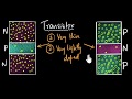
- يتكون من ثلاث مناطق رئيسية: الباعث (مشبع بشدة)، القاعدة (مخدرة قليلاً وضيقة)، والمجمع (مخدر بشكل معتدل وأوسع).
- يحتوي على تقاطعين PN بين المناطق.
مناطق تشغيل BJT
- المنطقة النشطة: باعث-قاعدة متحيز للأمام، قاعدة-مجمع متحيز عكسي، تُستخدم في التكبير.
- منطقة القطع: كلا التقاطعين متحيزان عكسيًا، يُستخدم كمفتاح مغلق.
- منطقة التشبع: كلا التقاطعين متحيزان للأمام، يُستخدم كمفتاح مفتوح.
- المنطقة النشطة العكسية: يقل فيها المكسب وغالبًا ما تُتجنب.
لمزيد من الفهم حول خصائص المناطق المختلفة للترانزستور، يمكن الرجوع إلى Understanding MOS Junction C-V Characteristics: Accumulation, Depletion, and Inversion لتحصيل شرح مكمل لمفاهيم الحيزات الكهربائية في أشباه الموصلات.
رموز الترانزستور
- يوضح اتجاه السهم في رمز NPN اتجاه التيار من القاعدة إلى الباعث.
- في PNP، يتجه السهم بالعكس.
تكوينات الترانزستور
- Emitter المشترك: إشارة الإدخال بين القاعدة والباعث، الإخراج بين المجمع والباعث.
- المجمع المشترك: المجمع مشترك بين الإدخال والمخرج.
- القاعدة المشتركة: القاعدة مشتركة بين الإدخال والمخرج.
عمل ترانزستور NPN في المنطقة النشطة
- تطبيق جهدي VBB للقاعدة وVCC للمجمع.
- باعث-قاعدة متحيز للأمام (VBE ~ 0.7 فولت)، وقاعدة-مجمع متحيز عكسي.
- تدفق الإلكترونات من الباعث إلى القاعدة، ثم إلى المجمع.
- الجزء الأكبر من الإلكترونات يمر عبر القاعدة لأن القاعدة ضيقة ومخدرة قليلاً.
العلاقات الكهربائية للتيارات
- العلاقة الأساسية: تيار الباعث = تيار القاعدة + تيار المجمع (IE = IB + IC)
- التيار IC يساوي تقريبًا α × IE حيث α قريب من 1.
- المعامل بيتا (β) يربط IC بـ IB (IC = β × IB)، ويتراوح عادة بين 50 و400.
- يمكن من خلال التحكم في تيار القاعدة التحكم في تيار المجمع.
الفروقات بين BJT وترانزستور تأثير المجال
- BJT هو جهاز تحكم في التيار.
- ترانزستور تأثير المجال هو جهاز تحكم في الجهد.
للمقارنة المفصلة مع مفاهيم التحكم في الطاقة والطاقة الداخلية في الأجهزة، يمكن الاطلاع على Understanding Internal Energy: Heat and Work in Thermodynamics لإثراء الفهم حول كيف تؤثر الطاقة على سلوك الأجهزة الإلكترونية.
خلاصة
- ترانزستورات BJT أساسية في الإلكترونيات لتضخيم الإشارة والتحكم في التيار.
- يتم استخدامها في تكوينات مختلفة حسب التطبيق.
- سيركز المحتوى القادم على خصائصها، التكوينات، وكيفية التحيز.
لمزيد من الأسئلة والتوضيحات، يمكنكم ترك تعليق أو الاشتراك في القناة لمتابعة الشروحات التفصيلية القادمة.
Hey, friends welcome to the YouTube channel ALL ABOUT ELECTRONICS. So in this video, we will learn about the Bipolar Junction Transistor. The invention of the transistor, led the invention of the many other semiconductor devices including the integrated circuits. And in fact, due to these
integrated circuits, the modern day computers, and other electronic gadgets, which we are using is possible. So the bipolar Junction transistor or the BJT is a three terminal semiconductor device, which can act as a conductor or insulator based on the applied input signal. And due to this
property, the transistor can be used as a switch in the digital electronics. Or it can be used as an amplifier, in the analog electronics. So nowadays, the field effect transistors, are widely used in the electronic industry. But still the BJTs are extensively used. And anyone
who is interested in the electronics, should have some basic knowledge of this BJT. So in this bipolar Junction transistor, there are three doped regions. The Emitter, the Base and the Collector. And based on the doping of these three regions, it is known as either NPN or PNP transistor. So
in case of the NPN transistor, both Emitter and the Collector are doped with the N-type impurity, and the Base is doped with the P-type impurity. On the other end, in the PNP transistor, the Base is doped with the N-type impurity, and the Emitter and the Collectors are dope with the P-type
impurity. And here, the term bipolar indicates that, both electrons and holes contributes in the flow of current. Now if you look inside this BJT, then there are two PN junctions. One is between the Emitter and the Base, and second is between the Base and the Collector. And it appears as if,
the two back-to-back diodes are connected in the series. But actually, it won't behave like that. Because when we connect to back-to-back diodes, then we are assuming that, there is no interaction between the two diodes. That means these two diodes are operating independently. But in
case of the BJT, actually there is an interaction between the two regions. So if we connect the two back to back diodes like this, then it won't behave like a BJT. Now if we talk about the internal construction of the BJT, then the Emitter is heavily doped, and the function of the Emitter
is to supply the electron. And in fact, that is why it is known as the Emitter. Then if you talk about the Base, then it is lightly doped, and the doping concentration of the Collector is between the Emitter and the Base. That means the Collector is the moderately doped. And if we talk
about the width of these three regions, then the Base region is much narrower, compared to the two regions. So in terms of the width, the Collector region is wider, than the other two regions. Because the job of the Collector region is to collect the electrons, which is supplied by
the Emitter. And in fact, that is why, it is known as the Collector. Now depending on the biasing, the BJT can be operated in three regions. The Active Region, the Cut-off Region and the Saturation Region. So in case of the Active Region of operation, the Emitter Base Junction, is
forward biased. and the Base Collector Junction is reversed biased. So let's say, the voltage at the Emitter is VE, the voltage at the Base is VB, and the voltage at the Collector is VC. And to forward bias this Base Emitter Junction, the voltage of Base should be greater than the Emitter. And
similarly, to reverse bias this Collector Base Junction, the voltage at the Collector should be greater than Base. That means, to operate the BJT, in the active region, we can say that, the Collector voltage should be greater than Base voltage, and the Base voltage should be greater
than Emitter voltage. So once this condition is satisfied, then the BJT will operate in the active region. Similarly, in the Cut-Off region both Base-Emitter junction and the Base Collector junctions are reversed biased. So to operate the BJT in this region, the Emitter voltage, should be
greater than Base voltage, and at the same time, the Collector voltage should also be greater than Base voltage. Similarly, in case of the Saturation Region of operation, both Base Emitter, and the Base Collector junction of the BJTs, are forward biased. That means in this region of operation,
the Base voltage VB is greater than Emitter voltage, and at the same time, this Base voltage, is also greater than Collector voltage. So these are the three regions of operation, in case of the BJT. Apart from that, there is a one more region of operation, which is known as the Reverse
Active Region of Operation. So in this region of operation, instead of Base Emitter Junction, here the Base Collector Junction is forward biased, and the Base Emitter Junction is reverse biased. But in this region of operation, the gain provided by the BJTs very less, and due to that, this region
of operation is usually avoided. Similarly, if we talk about the PNP transistor, then in case of the Active Region of Operation, this Base Emitter Junction is forward biased, and the Collector Base Junction is reverse biased. But in this case, now the Emitter voltage is greater than the Base
voltage, and similarly the Base voltage is greater than Collector voltage. So we can say that, in case of the PNP transistor, to operate it in the active region, the Emitter voltage should be greater than Base voltage, and the Base voltage should be greater than the Collector voltage.
And similarly, this PNP transistor can also be used in the different regions. So whenever, the BJT is used for the amplification, then it is used in this Active Region. And whenever it is used as a switch, and it is used in the Saturation in the Cut-off Region. And in the upcoming videos,
we will see in detail about these different regions of operation. Now if we talk about the symbol, then this is the symbol of the NPN transistor. So these three terminals, are the Base Collector and the Emitter. And here, this arrow indicates the direction of the current
during the Active Region of Operation. So in case of the NPN transistor, the current will flow from the Base towards the Emitter. On the other end, if you see the symbol of the PNP transistor, then it is similar to the NPN transistor, but here the direction of the arrow will get reversed. So now,
the current will flow from the Emitter towards the Base region. Now as I said, when the BJT is used for the amplification of the signal, then it is operated in the active region. And there are different ways to configure it. So in case of the common Emitter configuration,
the Emitter terminal is common between the input and the output. That means, in this configuration, the input signal is applied between the Base and the Emitter, and the output is measured, between the Collector and the Emitter terminal. Similarly in case of the common Collector configuration,
the Collector terminal is common between the input and the output side. And likewise in the common Base configuration, the Base terminal is common between the input and the output side. So each configuration has its own advantage and disadvantage, and we will see all these
configurations in detail in the upcoming videos. But in short, depending on the requirement, and the application, the BJT can be configured in any of these three configurations. All right, so now let's understand the working of the BJT, whenever it is operated in the active region.
And here, we will take the example of the NPN transistor. Now before we understand the working, let me just clear the notations, which is used for the supply voltages. So as you can see were here, for the Base and the Collector supplies, double subscription is used. That means here,
this VBB is a source voltage for the Base. And the VCC is the source voltage which is connected to the Collector terminal. And this voltage VBE defines the difference between the voltage at the Base and the Emitter terminal. So this voltage VBE can be defined as voltage VB minus VE. So if the
voltage at the Base terminal is let say VB and the voltage at the Emitter terminal is VE, then the voltage VBE can be defined as voltage VB minus VE. And here, this voltage VB and VE are measured with respect to the ground terminal. Similarly, this voltage VCE can be defined as the Collector
voltage VC minus VE. So instead of VBE if we write voltage VEB, then it can be written as voltage VE minus VB. And this voltage, will be negative of the VBE. So throughout our discussion on the BJT, we will use these notations. So here these Base voltage, and the Collector voltage, is applied
in such a way that, the base Emitter Junction will get forward biased. And the Base Collector Junction will get reversed bias. That means over here, the BJT is biased in such a way that, this voltage VBE is positive, and this voltage VCB is also positive. Now if you notice over here,
this is the PN Junction. So whenever this PN Junction is forward bias, and the typical photo voltage drop across this diode is in the range of 0.6 to 0.7 volt. That means, whenever we forward bias these Base Emitter Junction, then the typical voltage drop between these Base and the Emitter
Junction, will be roughly around 0.7 volt. Now once we apply this biasing voltages, and the electrons from the Emitter, will be pushed towards the Base terminal. Because as I said earlier, the Emitter is the heavily doped. That means the Emitter has the large number of electrons,
as the majority carriers. And once we apply the biasing voltage, then this negative voltage will push the electrons towards the Base region. So due to that, the electrons will starts moving towards the Base region. Now once the electrons enters this Base region, and there are two paths for
them. One is they can flow towards the positive terminal on the left, and the second is they can flow into the Collector region. But most of the electrons will enter into the Collector region. Because if you see over here, the Base is lightly doped. That means a number of holes in this Base
region, is very small compared to the electrons, which are coming from the Emitter region. That means the free electrons, which has come into this Base region will see the longer lifetime. And the second reason is, the width of this Base region is very thin. That means most of the electrons, will
be able to escape this Base region, and they can go into the Collector region. That means in this Base region, only few electrons will recombine with these holes, and they will be get attracted towards the positive terminal of this VBB. And the remaining electrons will enter into the Collector
region. Now, if you notice over here, once the electrons from the Emitter enter into the Base region, then they will become the minority charge carriers. And if you see over here, the Base Collector Junction is reversed biased. So due to the applied electric field at the Collector
terminals these minority charge carriers, or the electrons will get attracted towards the Collector terminal. So once the electrons enters into this Collector region, then they will get attracted by the positive terminal of this VCC. So if you see the direction of the flow of electron,
and from the emitter the electrons will flow in this direction, and most of the electrons which is emitted by the Emitter will get collected by the Collector region. And very small amount of electrons only will flow in this direction. And if we see the direction of the holes,
then it will be exactly opposite to the flow of electrons. And in fact, the conventional current, will also flow in the same direction. That means, the Base current IB will flow in this direction, while the Collector and the Emitter current will flow in this direction. So now let us establish
the relationship between all these currents. So if you apply the KCL, then we can say that this current IB plus IC, that is equal to Emitter current. That means the Emitter current is the summation of this Base current and the Collector current. As I said, only fraction of electrons,
are able to go in this direction. That means the Base current will be very small. Or we can say that, this Collector current IC, is approximately equal to IE. And exactly it can be defined as Collector current IC is equal to alpha times IE. And this alpha defines, what fraction of the
Emitter current is flowing through the Collector terminal. Now if we put this value of IC in this expression, then we can say that, this Base current IB plus alpha times IE is equal to IE. That means the Base current IB is equal to 1 minus alpha times Emitter current. And once again if we put
the value of IE in terms of the Collector current, then we can say that, the base current IB is equal to 1 minus alpha times IC divided by alpha. That means the Base current IB is equal to 1 minus alpha divided by alpha times Collector current. Or we can say that, the collector current IC is
equal to alpha divided by 1 minus alpha times Base current. And let's say this is equal to beta. That means the Collector current IC is equal to beta times IB. So this beta is known as the current gain of the BJT. And typically, the value of beta varies from 50 to 400 for the different
transistors. So from this we can say that, IB plus IC that is equal to Emitter current. That means Base current IB plus beta times IB is equal to IE. That means the Emitter current IE can be given as beta plus 1 times IB. So this is the relationship between the Base current, Emitter current
and the Collector current. Now if you notice over here, in this common Emitter configuration, this Base current is the current on the input side, while the Collector current is the current on the output side. And these two currents, are related by this expression. That means by controlling this
Base current on the input side, it is possible to control the collector current. And that is why, these Bipolar Junction Transistors are known as the current control device. That means just by controlling the input current on the Base side, it is possible to control the output current.
On the other end, if you see the other type of transistor, that is the field effect transistor it is the voltage control device. That means in that case, by controlling the input voltage, it is possible to control the output current. Also if you notice over here, in this configuration of
the BJT, the output collector current gets amplified by the factor of beta. And if we connect the resistor between the Collector and the Emitter terminal, then it is possible to amplify the input signal. That means after biasing by BJT, in this configuration, if we apply the AC signal
at the input, then it is possible to amplify that signal. And we will discuss about it in the detail in the upcoming videos. Now during our discussion, we haven't considered the current due to the minority charge carriers in this collector region. Because if you notice over here, this Base
collector Junction is reversed bias. So for a moment, if we remove this Emitter connection, then the current which is flowing through the Collector is only due to the minority charge carriers. And let's say, this current is equal to IC O. So this current is similar to the reverse
saturation current, which we have seen in the PN junction diode. So the total Collector current ICT will be equal to the IC plus ICO. Where this ICO is the current due to the minority charge carriers. And typically this current is in the range of microamperes. While this Collector
current IC is in the range of milliampere. So this is all about the different types of currents in the BJT. So in the upcoming videos, we will see the different configurations of the BJT, as well as the input and output characteristics of the BJT. And we will also see, how the BJT can be
biased using the different techniques. But I hope in this video, you got a brief overview about the BJT. So if you have any question or suggestion, do let me know here in the comment section below. If you like this video hit the like button, and subscribe the channel for more such videos.
ترانزستور ثنائي القطب (BJT) هو جهاز شبه موصل ثلاثي الأطراف يمكن استخدامه كمفتاح إلكتروني أو كمكبر للإشارات. يعمل عن طريق التحكم في تيار القاعدة الذي يؤثر على تيار المجمع، مما يسمح بتضخيم أو تبديل الإشارة داخل الدائرة.
ترانزستور NPN يتكوّن من طبقتين من نوع N بينهما طبقة من نوع P، بينما PNP يحتوي على طبقتين نوع P تفصل بينهما طبقة من نوع N. في NPN، يتحرك التيار من المجمع إلى الباعث، وفي PNP يكون التيار في الاتجاه المعاكس. ويختلف اتجاه السهم في الرموز التعبيرية لكلا النوعين.
تشغيل BJT يعتمد على تحيز التقاطعين PN: في المنطقة النشطة يكون باعث-قاعدة متحيز للأمام وقاعدة-مجمع متحيز عكسي للتكبير. في منطقة التشبع، يكون كلا التقاطعين متحيزين للأمام مما يسمح بمرور تيار كبير ويستخدم كمفتاح مفتوح. في القطع، يكون كلا التقاطعين محايدين أو متحيزين عكسيًا ولا يمر التيار.
العلاقة الأساسية هي أن تيار الباعث (IE) يساوي مجموع تيار القاعدة (IB) وتيار المجمع (IC) أي IE = IB + IC. التيار IC مرتبط بتيار الباعث بمعامل α (قريب من 1)، كما يربط المعامل β بين تيار المجمع والقاعدة حيث IC = β × IB، وعادة ما يتراوح β بين 50 و400.
هناك ثلاث تكوينات رئيسية: الباعث المشترك حيث تكون الإشارة الداخلة بين الباعث والقاعدة، والمجمع المشترك حيث يكون المجمع مشتركًا بين المدخل والمخرج، والقاعدة المشتركة حيث تكون القاعدة مشتركة. كل تكوين يؤثر على الكسب والمقاومة والاستجابة الترددية للترانزستور وفقًا للتطبيق المطلوب.
ترانزستور BJT هو جهاز تحكم في التيار حيث يتم التحكم بتيار القاعدة للتحكم بتيار المجمع، أما ترانزستور تأثير المجال (FET) فهو جهاز تحكم في الجهد حيث يتم التحكم في تيار القناة بواسطة جهد البوابة بدون مرور تيار عبرها، مما يجعله أكثر كفاءة في بعض التطبيقات.
لتشغيل ترانزستور NPN في المنطقة النشطة، يجب تطبيق جهد موجب على القاعدة بالنسبة للباعث (حوالي 0.7 فولت) لتحفيز باعث-قاعدة للأمام، ويكون جهد المجمع أعلى من الباعث لتحفيز قاعدة-مجمع عكسيًا. ينتج عن ذلك تدفق الإلكترونات من الباعث عبر القاعدة باتجاه المجمع، مما يسمح بتضخيم التيار.
Heads up!
This summary and transcript were automatically generated using AI with the Free YouTube Transcript Summary Tool by LunaNotes.
Generate a summary for freeRelated Summaries

شرح مبسط لعمل الاتصالات اللاسلكية وموجات الراديو
يقدم الفيديو شرحًا تفصيليًا لكيفية إرسال الرسائل عبر الإنترنت من خلال الهواتف المحمولة واستخدام موجات الراديو، موضحًا دور الهوائيات، الموجات الكهرومغناطيسية، والأبراج الخلوية، إلى جانب الفرق بين الاتصالات اللاسلكية والكابلات الأرضية.

شرح شامل لأنواع المتشكلات الكيميائية وتفاعلات الكيمياء العضوية
يغطي الفيديو أنواع المتشكلات البنيوية والفراغية بالإضافة إلى المتشكلات الضوئية وتأثيرها في الكيمياء العضوية. كما يستعرض التفاعلات الأساسية مثل إضافة الكتروفيل والاستبدال النيوكليوفيلي مع أمثلة تفصيلية على تسميات المركبات وتفاعلات الأرينات.

شرح مبسط لحركات قطع الشطرنج الأساسية واستخداماتها في اللعب
في هذا الفيديو التعليمي، يقدم إسلام حماده شرحًا تفصيليًا لحركات قطع الشطرنج الرئيسية مثل الروك، الفيل، الوزير، الحصان والملك، مع تقديم قواعد مهمة لفهم كيفية تحرك كل قطعة وأهميتها في اللعبة. يُمكن للمتعلمين من جميع المستويات الاستفادة من هذا الشرح المبسط الذي يعتمد على أساليب تعليمية عملية وتمارين تفاعلية تعزز من مهارات اللعب.

فهم الانقسام المنصف: العملية التي تخلق التنوع الوراثي
في هذا الفيديو، نتناول عملية الانقسام المنصف وكيف تساهم في تكوين الأمشاج والتنوع الوراثي بين الأشقاء. نوضح الفرق بين الانقسام المنصف والانقسام المتساوي، ونستعرض المراحل المختلفة للانقسام المنصف وتأثيرها على الكروموسومات.
Как работи транзисторът като усилвател на звук
Това видео обяснява как транзисторът преобразува малки електрически сигнали от микрофон в усилен ток, който може да захрани говорител и да възпроизведе звук с по-голяма сила. Разглеждаме структурата на npn транзистора и процеса, чрез който малък ток управлява голям ток, с подробно обяснение на електронните процеси в него.
Most Viewed Summaries

A Comprehensive Guide to Using Stable Diffusion Forge UI
Explore the Stable Diffusion Forge UI, customizable settings, models, and more to enhance your image generation experience.

Kolonyalismo at Imperyalismo: Ang Kasaysayan ng Pagsakop sa Pilipinas
Tuklasin ang kasaysayan ng kolonyalismo at imperyalismo sa Pilipinas sa pamamagitan ni Ferdinand Magellan.

Mastering Inpainting with Stable Diffusion: Fix Mistakes and Enhance Your Images
Learn to fix mistakes and enhance images with Stable Diffusion's inpainting features effectively.

Pamamaraan at Patakarang Kolonyal ng mga Espanyol sa Pilipinas
Tuklasin ang mga pamamaraan at patakaran ng mga Espanyol sa Pilipinas, at ang epekto nito sa mga Pilipino.

How to Install and Configure Forge: A New Stable Diffusion Web UI
Learn to install and configure the new Forge web UI for Stable Diffusion, with tips on models and settings.

If you found this summary useful, consider buying us a coffee. It would help us a lot!